Facebook
 Google
 GitHub
 Linkedin
Super Junction N-Channel MOSFETs for High-Voltage, Fast-Switching
Central Semiconductor’s 650 V Super Junction N-Channel MOSFETs are designed to deliver power conversion efficiency in high-voltage, high-frequency switching applications.
Central Semiconductor has introduced five 650 V Super Junction N-Channel MOSFETs designed for high-voltage, power-dense power conversion circuits in electric vehicle (EV) charging, renewable inverters, power factor correction, and switch mode power supply (SMPS) applications.

EV charging. Image used courtesy of Adobe Stock
The high-voltage MOSFETs are available in TO-220FP packaging and support operating currents as high as 29 A, with on-resistances (RDSON) as low as 130 mΩ for efficient and cost-effective high-power conversion.
Based in Hauppauge, New York, Central Semiconductor has built a business (since the 1970s) focused partly on supporting trailing-edge semiconductor technologies in legacy packages. This allows OEMs to extend the life of their product platforms without the need for costly redesigns.
EV Onboard Charging Applications
Level 1 and Level 2 EV chargers provide single or multi-phase AC power to an EV’s onboard charger (OBC). Within the EV, the OBC provides rectification and power factor correction of the input AC power, followed by an isolated DC-DC converter that generates high-voltage DC for charging the EV battery pack.
.jpg)
EV charging with AC power (Levels 1 and 2). Image used courtesy of Central Semiconductor
Central Semiconductor currently offers a robust portfolio of silicon and silicon carbide (SiC) diodes, rectifier modules, and MOSFETs suitable for EV charging applications, and the new 650 V devices are an expansion to this selection.
According to Tom Donofrio, director of Marketing and Sales Operations at Central Semiconductor, the high-voltage MOSFETs will extend Central’s portfolio of fast-switching devices and pair well with the company’s HyperFast Rectifiers used in PFC circuits for EV charging and similar applications.

Central Semiconductor products for EV charging. Image used courtesy of Central Semiconductor
At $1.25 each in low volumes, the silicon MOSFETs are a good lower-cost alternative to more exotic wide bandgap solutions like SiC or gallium nitride (GaN). Still, the Super Junction MOSFETs deliver performance, supporting power-dense designs with high-speed switching capabilities (up to 1 MHz) and low on-resistances.
Driving a Silicon MOSFET
In a semiconductor, the energy needed to transition electrons from the valence to the conduction band is known as the bandgap. For FETs, this translates to the voltage (energy) required to transition the device to an ON state.

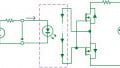
CDMSJ22029-650 drive characteristics. Image used courtesy of Central Semiconductor
Emerging SiC and GaN devices are important technologies for high-voltage, power-dense conversion circuits due to their higher switching speeds, low loss conduction, and reliability at high temperatures. However, the higher bandgaps of these compound semiconductors, as measured in electron volts (eV), can make them more difficult to operate.
Conversely, silicon FETs with lower bandgaps are much easier to operate, allowing for simpler gate drive circuits. The gate-source threshold voltage (VGS(th)) is the voltage required to induce a conduction channel in a FET. For the CDMSJ22029-650, this value is just 3 V.