Facebook
 Google
 GitHub
 Linkedin
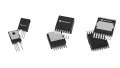
Infineon Introduces ThinPAK 8 x 8 Leadless SMD Package for HV Power MOSFETs
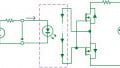
Infineon Technologies introduces the ThinPAK 8 x 8, a new leadless SMD package for HV MOSFETs. The new package has a very small footprint of only 64mm² (vs. 150mm² for the D2PAK) and a very low profile with only 1mm height (vs. 4.4mm for the D2PAK). According to the company, the significantly smaller package size, combined with benchmark low parasitic inductances, provides designers with a new and effective way to decrease system solution size in power density driven designs.
The new 1mm-high surface-mount package houses the industry-standard TO-220 die size within a leadless outline measuring only 8 x 8mm and features an exposed metal drain pad for efficient removal of internally generated heat. Its low profile will enable designers to achieve slimmer power supply enclosures enabling compact and stylish new products for today’s markets.
This new standard is available from two companies: Infineon and ST will introduce MOSFETs using this package, which is named ThinPAK 8x8 by Infineon and PowerFLAT™ 8x8 HV by ST, therefore providing customers with a high-quality alternative source.
"This type of package sets a new market standard for leadless SMD packages for HV MOSFETs, and is being introduced today in co-operation with S™icroelectronics," said Jan-Willem Reynaerts, Product Line Manager HVMOS Power Discretes at Infineon Technologies. "Silicon technologies like CoolMOS™ have reached such an advanced stage of fast and efficient switching, that the standard traditional through-hole packages more and more have become the limiting factor in getting to the next level of energy efficiency and power density."
The ThinPAK 8 x 8 package is characterized by a very low source inductance of only 2nH (vs. 6nH for the D2PAK), a separate driver source connection for clean gate signals, as well as a thermal performance similar to the D2PAK. As a result, the ThinPAK 8x8 package enables faster and thus more efficient switching of Power MOSFETs and is also easier to handle in terms of switching behavior and EMI.
Infineon will initially offer three 600V CoolMOS™ devices in the new package: 199mΩ (IPL60R199CP), 299mΩ (IPL60R299CP) and 385mΩ (IPL60R385CP).
Qualification samples of the new devices in ThinPAK 8 x 8 packages are now available, with production volumes available against forecast within standard lead times.