Facebook
 Google
 GitHub
 Linkedin
GaN Systems and Silanna Semiconductor Release ACF Charger Reference Design
The new design is for a highly efficient, 65 watt active clamp flyback charger targeted at USB-C power delivery (PD) applications
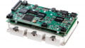
The GaN-based 65W Active Clamp Flyback (ACF) charger reference design is available from Silanna Semiconductor. It is designed to be implemented on Silanna’s SZ-RD12-65W evaluation board (EVB). The collaborative design demonstrates a practical design for a GaN-based ACF USB PD charger, and will serve to reduce both the BOM count as well as time to market for OEMs.

From left to right, top and bottom sides of the SZ-RD12-65W Evaluation Board. Image courtesy of Gan Systems
About the new ACF Design
ACF circuitry generally requires two FETs in low-side and high-side and in low-side configuration. This design employs Silanna Semiconductor’s SZ1130 ACF Pulse Width Modulator (PWM) controller, which incorporates the high-side FET within itself. The design also incorporates GaN Systems’ GS-065-008-1-L 650V GaN power transistor and a standard RM8 transformer.
The new charger design achieves an impressive power density of 30 watts per cubic inch with a peak efficiency of better than 94%. Component temperatures stay below 95℃, and great EMI design results in close to no ringing or voltage spikes.
The design accommodates inputs ranging from 90 to 265 VAC, and the following outputs are supported:
- 5V at 3 amps
- 9V at 3 amps
- 15V at 3 amps
- 20V at 3.25 amps
As per Jim Witham CEO of GaN Systems, “Silanna Semiconductor’s SZ1130 chip is a great fit for 65W ACF designs and is another example of a company developing an innovative solution in recognition of the growing importance of GaN to power engineers.” He goes on to say that, “As GaN becomes the standard building block across markets, it's good to see that the ecosystem continues to grow.”
The SZ-RD12-65W Evaluation Board
Silanna’s SZ-RD12-65W is described in its Evaluation Report. The device employs GaN Systems’ GS-065-008-1-L (650 V E-mode GaN Transistor) along with Silannna’s SZ1130. The EVB serves to demonstrate the coexistence of efficiency and high power density that can be achieved, due to its high level of integration of the SZ1130 flyback PWM controller.
The GS-065-008-1-L
The GS-065-008-1-L, described in its datasheet, is a 650 V enhancement-mode GaN-on-silicon power transistor with a maximum IDS of 8 amps. It boasts an RDS(ON) of 225 mΩ and a total gate charge (QG) of 1.6 nC, for an “ultra-low” figure of merit.
The unit features a simple gate drive requirement of 0 to 6 volts, and it can switch at frequencies in excess of 1 MHz. It is a bottom-side cooled transistor that offers a junction-to-case thermal resistance of 2 ℃/watt.
The GS-065-008-1-L is:
- Available in a 5 x 6 mm PDFN package
- Operates over a temperature range of -55 to +150℃
- RoHS 3 (6+4) compliant
Silanna Semiconductors’ SZ1130
Silanna Semiconductor’s SZ1130 is a Flyback PWM Controller with Integrated Active Clamp Circuit. Texas Instruments presents a short video explaining the operation of the active clamp flyback, and it’s by incorporating more of this function within one IC that the SZ1130 achieves its utility.

Basic application diagram for the SZ1130 active clamp flyback controller. Image courtesy of Silanna
The SZ1130 employs Silanna’s OptiMode TMdigital control architecture, by means of which it can adjust the device’s mode of operation on a cycle-by-cycle basis. This makes it possible, even in response to varying line and load conditions, to still maintain high efficiency, low EMI, and fast dynamic load regulation.