Facebook
 Google
 GitHub
 Linkedin
Alpha and Omega Semiconductor Launches New Ground Exposed Die Pad Power IC Platform
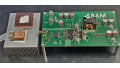
Alpha and Omega Semiconductor Limited (AOS) introduced its new Ground Exposed Die Pad Power IC platform, an innovative packaging technology capable of exceptional power dissipation. The high performance of this EZBuck™ dc/dc platform is attributed to a combination of IC design, low on-resistance MOSFET technology, and proprietary exposed ground pad packaging technology. The new platform enables more thermally efficient dc/dc solutions for consumer, networking and industrial applications such as LCD TVs, set-top boxes, cable modems, and power supplies.
The ground exposed die pad platform combines a current-mode step-down controller IC with integrated high-side and low-side MOSFETs. The vertical MOSFET structure features outstanding on-resistance performance which allows more power delivery in a small area, while the exposed ground pad transfers heat directly to the printed circuit board's ground plane which acts as a large heat sink. Another benefit of the large ground exposed pad is that it reduces electromagnetic interference and noise coupling into the system.
The high-side p-channel MOSFET and low-side n-channel MOSFET with integrated Schottky diode, combined with a bond-wireless packaging technology deliver best-in-class junction temperature performance for a 30W, 12V to 5V post-regulating application.
"The integration of the discrete FET technology and the exposed ground pad are significant features for future EZBuck products, which will offer higher power density without the added cost," said Daniel Chang, Vice President of Power IC at AOS.
The first EZBuck products with the new featured platform will be available within the first quarter of 2013.