Facebook
 Google
 GitHub
 Linkedin
Partnering in SiC MOSFETS to Deliver Automotive and Industrial Solutions
An interview with Dr. Rainer Käsmaier about SiC-based products in the rapidly growing power semiconductor market.
Interview with Dr. Rainer Käsmaier, ABB
To accelerate market entry into the high-growth electric vehicles (EV) sector, Dr. Rainer Käsmaier, Managing Director of Semiconductors at ABB’s Power Grids business, and Gregg Lowe, CEO of Cree, the leading US-based manufacturer of silicon carbide power semiconductors, have announced a partnership to jointly expand the rollout of SiC-based products in the rapidly growing power semiconductor market. This contract is to enable Cree to broaden its customer base, leveraging ABB’s extensive power semiconductor portfolio.
By incorporating Cree’s silicon carbide semiconductors into its product portfolio, ABB accelerates its entry into the fast-expanding EV sector.
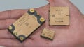
For Cree, the partnership enables the company to broaden its customer base. Cree’s products will be included in ABB’s power semiconductor product portfolio, across power grids, train and traction, industrial, and e-mobility sectors. Cree’s high-end silicon carbide devices will be assembled into power modules in ABB’s award-winning automated power semiconductor factory in Lenzburg, Switzerland.

We have asked Dr. Käsmaier some questions about the partnership with Cree:
What was the main reason for you to make this arrangement with Cree?
The main reason was essentially that we at ABB decided some time ago that the expertise we have in the high-voltage (HV) area of semiconductors would enable us to open new business areas. This is exactly in line with the trend in electric cars, requiring HV power semiconductors to drive electric motors and to charge HV battery systems. In this market – in addition to industrial and rail markets in which our semiconductors have already been in use so far – we have exactly the appropriate experience to use and apply our expertise, and wide bandgap (WBG) technology, in this case, SiC, is an efficient base material option for the EV applications.
We have been developing power components for quite some time that are also well suitable for use in vehicles. It was also foreseeable that silicon carbide would bring significant advantages in the electric vehicle power train and that we would, therefore, have to deal with it. And here Cree virtually offers itself as a strong partner.
But you already had power modules in your portfolio?
That's right. Power modules are the main products in our Semiconductors product group, and they go into various markets. Essentially, we have been providing our power modules in all industrial segments requiring voltage source converters. We are particularly well on our way in the large traditional “mobility” segment of traction inverters for trains.
And, of course, we are very active in delivering semiconductor modules for Power Grids, our home division. With renewable power grids, it's becoming extremely important to transport bulk electricity from wind or solar power plants – which are located somewhere, but not exactly where the cities are – over long distances. Highly efficient substations are needed for that purpose (which my colleagues in another ABB division will then build).
And it's precisely this know-how that we have that can also be used very well in the automotive sector. Automotive power modules naturally look different from that of a train or an HVDC converter station. Requirements in terms of size, form factor, and converter integration are different in a car. We believe that we have understood these requirements very well and we presented such a module at PCIM.
Your move in the direction of wide bandgap silicon carbide in this respect is also beneficial for the environment because of its smaller dimensions, higher efficiency and reliability, and lower consumption?
At ABB, we are not on the road with lower voltage silicon MOSFET or gallium nitride, but in the higher voltage segment. We see the need to use SiC in order to contribute to environmental friendliness and reduced battery sizes. Compared to a standard silicon-based semiconductor, a silicon carbide semiconductor allows energy conversion with almost no losses, thus reducing power conversion losses and carbon dioxide emissions.
But this can in future also open options for the rail sector, where our modules are used in high-speed trains all over the world offering an attractive alternative to flight operations – a considerable contribution to the increased cleanliness of our planet. This has an even greater effect in Asia with its long distances, but it´s also becoming more and more important in Europe.
For EVs, whose customers are the end consumers, you need a small power electronics unit that consumes little electricity allowing to maximize the driving range with the existing battery, or – which is a burning issue – use a smaller battery with a correspondingly lower weight and cost. If you can then make everything that consumes electricity and is necessary for electricity conversion more efficient, then you can also achieve the desired longer range, which is still a decisive purchase criterion for any electric car.
Were you already active in the wide-bandgap business before this partnership announcement?
Yes. We have been developing silicon carbide as a research topic for several years now and presented the above-mentioned first prototypes of a SiC-based module for electric cars at the PCIM. Of course, you must always distinguish between the module and the SiC chip, which represents only one, albeit essential, step in the entire module.
Yes, I am very proud of Jürgen Schuderer and the whole research team, and it was essential that we started this research topic just in time a few years ago. With these results, we can now move into the industrialization phase and apply our know-how. If we were to start research now, we would be very late, if not too late.
Does this already go into packaging?
Yes, we now do the assembly part at our plant in Lenzburg, Switzerland. When we discovered that the research results were so promising, we started building up the capability to produce the module we presented at PCIM.
Is your agreement with Cree limited to SiC-MOSFETs, or does that go further into the basic development of WBG semiconductors?
It is well known that Cree not only makes MOSFETs, but also the step before, where they provide the wafer. They're really at the forefront of that – remember the announcement of a large investment in a SiC wafer factory by Gregg Lowe in Nuremberg in May. This proofs that Cree is a player who is very serious about all this: exactly the kind of partner we want.
Our partnership includes both wafers and MOSFETs: What Cree is also interested in is that we have know-how both for the MOSFET chips and for the next step, the modules. But we don't start from scratch. We had joint development projects even before this announcement.
It is quite possible that we will not only maintain the status quo that everyone has but also look at how we are progressing in the partnership in the future. Especially for our industry, you need to do developments constantly to stay competitive. And this is probably even more extreme in the semiconductor industry than in other industries because of the short cycle times.
This has been the case for decades. And if you then have a partner who is traveling a lot around the world, then it's also clear that you're tuning the development plans of both sides. The definition in detail is always a matter of alignment, but joint progress is very well planned.
Are there any links to other Cree contract partners such as ZF or Danfoss?
In general, companies like Cree cannot afford to cooperate with only one supplier in the high-voltage power semiconductor sector. The only important thing is that you know exactly that what you are discussing with this partner is separated from what is discussed with others. Of course, this professional behavior applies to both sides.
The exciting thing about this market is that many people are just starting out and it is not clear who is setting which focuses on where and who has to enter into partnerships with whom. For some, this is already apparent, for others it will only become apparent in the future.
So, it's all still in the flow?
The supply chain wafer – MOSFETs – modules – inverters must be built up first. For me, the best classic customer is one who builds an inverter. As a side remark irrelevant for our topic, just think of the area of autonomous driving - there are old players and newcomers, and nobody can say today who will have long-term success, who will be a customer and who will be a competitor.

Are you also contributing to ABB`s "Ability" platform?
Not directly. But we use it, we are internal customers, so to speak. And that's what I am happy to tell you: I'm sure you've noticed that our facility won the "Factory of the Year" award for automation last year because we fully automated the backend module line, of course with ABB robots. There are software solutions from ABB in use, and that has already helped us a lot to be able to access in-house solution offers.
The industrial sector is also an important area of application for the modules you offer, isn't it?
Of course. For a few years, we focused on Industry 4.0, on two tracks: As a self-user of Industry 4.0 as well as a provider of solutions for Industry 4.0. As a semiconductor manufacturer, we need both tracks, one of which is automation, for which we were awarded because we are able to fully control the module manufacturing from outside of the line.
The other area is the semiconductor in itself. As it becomes more intelligent, it can also enable intelligent and autonomous systems that are controlled, powered and moved. We are focusing on both and are organized accordingly to always stay up to date at the cutting edge. Else we would miss the train!
Brief Summary of the award-winning paper mentioned in the interview with Dr. Käsmaier:
High-Power SiC and Si Module Platform for Automotive Traction Inverter
Jürgen Schuderer et al. from ABB Corporate Research and Andreas Apelsmeier from AUDI AG, Germany
Abstract: A novel power semiconductor module platform for the automotive powertrain is presented in this paper. Mold modules are designed for symmetric and minimized parasitics by applying alternating and multilayer current routing. All interconnects are solder-free to provide superior reliability, and to meet present and future automotive requirements, e.g., passing 1000 temperature shock cycles in the range of -40 to 150 °C. SiC or Si devices are packaged in the same external outline offering simple scalability for inverter classes in the 150 – 350 kW power range. A screw-less and O-ring-less 3-phase inverter module is achieved by a laser welding of the mold modules to a low-cost Al cooler enclosure.
The rapid growth of electric vehicles presents the need for cost-effective and reliable power electronics inverters in the drive train of passenger and commercial vehicles. At the heart of the traction inverter are power semiconductor modules that control motor torque and speed via pulse width modulation.
These modules must fulfill specific requirements:
- Cost reduction is a key development target.
- Modules must be optimized for mechanical integration into highly compact inverters that are mounted in space-restricted engine compartments.
- Modules must be optimized for harsh environmental conditions.
To address these performance requirements, ABB has developed a SiC/Si power module platform with the following key features:
- A mold module approach is selected that does not require any housing (cost-benefit) and that provides excellent environmental protection, cycle reliability, and protection against shock, vibration and handling damage.
- A completely solder-free power module is realized for the highest cycle reliability and robustness standards. All interconnections are either sintered or welded. In addition, the device topsides are bonded by copper wire.
- To allow for SiC fast switching, power and gate loop parasitic inductances and coupling coefficients are rigorously minimized.
- A low-cost cooler enclosure is realized by laser welding of mold modules into a cooler structure based on embossed aluminum sheets. In this manner, a compact three-phase inverter module is achieved without the need for screwing or clamping of O-ring sealings.
- The module offers several aspects of scalability. Two different substrates are applied to assemble either a high-power SiC or a lower-power Si version for the identical external outline. This allows for output power scaling in the range of 150 – 350 kW. In addition, the module cost can be scaled by applying different power module component materials (substrates, baseplates, bond materials) to optimize for the right cost-performance ratio for the specific target vehicle.
- Module characterization and accelerated stress tests are conducted to validate the performance and to demonstrate high-temperature operation up to junction temperatures of 200 °C.
About the Author
Roland R. Ackermann has been a technology journalist since 1957, covering electronics, engineering and manufacturing/automation. He has been a freelance journalist in 1996, publishing work in Elektronik Journal, was editor in chief of Electronik Embedded System and verlagsweltMAGAZIN, and also wrote numerous articles in German and English publications and newspapers. He was a regular column writer in E&E Faszination Elektronik and is now a correspondent for Bodo's Power Systems. Ackermann holds talks at international venues, moderates panel discussions, and organizes events.
This article originally appeared in the Bodo’s Power Systems magazine.