Facebook
 Google
 GitHub
 Linkedin
Seven Steps to Highly Effective GaN Designs
Today, we operate in a very fast-moving world, looking for shortcuts, opportunities to “copy and paste” to complete tasks in a short period of time. Although GaN power transistors are relatively new, design “rules of thumb” have been established and proven to meet fast time-to-market objectives. Over the years, seven steps to a successful design have been developed and proven – backed by ongoing and updated documentation and customer training.
This article provides an overview of these seven steps and links to application notes to inform users and customers of the latest information needed to optimize their GaN designs.
Step 1 – Gate Drive Selection
Driving the gates of GaN enhancement mode high electron mobility transistors (E-HEMTs) has similarities in common with driving the gates of silicon (Si) MOSFETs – but with a few beneficial differences.
Driving GaN E-HEMTs does not eliminate any popular Si gate drivers; they simply make GaN easier and more effective to use. This means high-voltage (>600V) quasi-resonant and fixed frequency flyback adapters, chargers, and other low-power AC/DC controllers can be used for different LLC and power factor correction (PFC) configurations in GaN designs.
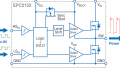
Simple circuitry provides the transition capability for using a Si controller for GaN devices. For a single GaN device, the isolated, negative VGS(OFF) EZDrive® circuit is a low-cost, easy way to use a 12V driver to drive a 6V GaN transistor for use with any controller or driver with single, dual, or high-side/low-side drivers. A new driver, the Heyday HEY1011, provides significant size reduction and board space savings in GaN designs. With its ability to eliminate bootstrap and isolated supplies, it is also the smallest isolated gate drive solution in the market. Figure 1 shows an evaluation board using a HEY1011 with an integrated power rail.

Figure 1. The GS EVB HB 66516B HD, a 650 V GaN E-Mode half-bridge evaluation board, features a HEY1011 L12C gate drive solution. Image used courtesy of Bodo’s Power Systems
Step 2 – Topology and Schematic Review
Designers need to constantly be on the lookout for the newest products since using an available, compatible controller simplifies the GaN designer’s task. Depending on the desired topology, such as critical conduction mode (CrM) or continuous conduction mode (CCM), an appropriate controller may already exist and be part of an evaluation tool. For example, an onsemi NCP1680 CrM analog bridgeless totem pole (BTP) PFC controller used in a 300W GaN evaluation demo board shown in Figure 2 results in high efficiency. As illustrated, 99% efficiency was achieved at full load at the highest (265V) voltage (plus, the controller’s design includes features for more efficient operation under light loads.)

Figure 2. A BTP PFC controller offers thermal and power density advantages over a boost PFC topology. Image used courtesy of Bodo’s Power Systems
Step 3 – Power Loss Calculation
Applying simple calculations can make the novice or experienced GaN designer more comfortable with using new technology. For example, in the application note “GaN Switching Loss Simulation using LTSpice” (GN008), a half-bridge double-pulse test circuit in LTSpice, is used as the test bench to evaluate switching performance under different electrical parameters. In the paper, the simulated switching losses are compared with lab measurements to verify the accuracy and suitability of the process. Additionally, “Modeling the Thermal Behavior of GaNPX® packages” (GN007) explains how RC thermal models found on GaN product pages can be used to perform detailed thermal simulation using SPICE. The App Note describes how to use the four-layer GaNPX package’s RC model in a SPICE simulation. A simple boost converter circuit is used to verify the functionality of the RC thermal model.
Step 4 – Layout Considerations
Since GaN E-HEMTs switch much faster than Si MOSFETs, they require proper engineering considerations for printed circuit board (PCB) layout design to minimize parasitic inductance issues. Specifically, parasitic inductances can cause higher overshoot voltages, ringing/oscillation, and electromagnetic compatibility (EMC) issues, which can lead to overstressing the E-HEMTs.
The application note “PCB Layout Considerations with GaN EHEMTs” (GN009) provides an overview of best engineering practices for PCB layout of designs using embedded GaNPX-packaged E-HEMTs. Layout guidelines are introduced for the following four circuit configurations:
- Isolated gate driver circuit for single GaN E-HEMTs
- Isolated gate driver circuit for paralleled GaN E-HEMTs
- Half-bridge bootstrap gate driver circuit
- EZDrive circuit
Optimum board layout combined with low package inductance enables GaN E-HEMTs to exhibit optimum switching performance.
Step 5 – Circuit Test Validation
GaN E-HEMTs have very low parasitic parameters. However, without proper care, the parasitic elements introduced by test equipment and measurement techniques, especially operating at higher frequencies, can overshadow the GaN device parameters and lead to erroneous measurement results.
Application note “Measurement Techniques for High-Speed GaN E-HEMTs” (GN003) explains the importance of measurement techniques and provides examples in several areas. Also, it discusses the Double Pulse Switching Test used to characterize hard switching turn-on and turn-off, including the Switch Test Setup and an example of test results. GaN Systems routinely tests Double Pulse Testing on every design we do and every customer we support. There is no better way to verify a good layout.
For switching energy, Eon/Eoff measurement probing techniques to increase measurement accuracy of VGS, VDS, and IDS are described, including switching loss distribution of GaN E-HEMTs and an Eqoss measurement example.
Step 6 – Thermal Design Optimization
Good thermal design is essential for power-handling devices such as GaN transistors. Improved thermal capabilities can be obtained using an insulated metal substrate (IMS) instead of an FR4 PCB. Compared to FR4 PCB heat transfer, the IMS design reduces the heatsink volume for high-power applications. Figure 3, from GN002, Thermal Design for Packaged GaNPX® Devices, depicts different (increasingly better) cooling techniques, including top cooling. As shown, when using high-performance GaN devices (both lower RθJA and lower on-resistance and parallel devices), much lower power losses and higher power operation can be achieved. In addition, SPICE (LTSPICE/PSPICE) and PLECS models can assist the system designer to optimize thermal and electrical performance.

Figure 3. Several design changes can increase the power-handling capability while significantly reducing the heatsink to ambient thermal resistance (RθHSA) in a specific GaN design. Image used courtesy of Bodo’s Power Systems
The new IEC 62368-1 hazard-based product-safety standard (replacing IEC 60950) reduces maximum touch temperature requirements, adding challenges in traditional thermal designs. While heat transfer improves with horizontal heat spreaders, vertical thermal conduction has become critical. An optimized thermal stack can include an advanced, 0.2 mm, thermal interface material (TIM), 3-mm copper shielding, and a 5-mm copper slug to achieve the lowest RθJA.
Step 7 – Electromagnetic Interference (EMI) Avoidance
The perennial power electronics issue – if not dealt with properly in the design – is EMI and EMC. In general, GaN technology helps reduce EMI due to Zero Reverse Recovery but controlling drive parameters is essential to control EMI. Also, copper shielding is recommended for EMI compliance. However, layout is the most important way to minimize EMI, and this final step reiterates considerations in Step 4.
Two reference designs bring out important circuit aspects to avoid EMI problems. One is a 65W Type-C USB Power Delivery (PD) quasiresonance (QR) charger, which addresses EMI for CISPR22 Conduction and Radiation Class B compliance. The second reference design is a 100W PFC QR USB PD charger with two Type C ports with EMI capability to pass EN55032 Class B with >6dB margin.
The Next Step – Ship the product!
Seven is the lucky number for GaN designs and design engineers --- if they follow the steps presented here – which offers a great overview of maximizing performance success. To dive deeper into each step, review the list of application notes at the end of this article. Additionally, the GaN Systems website provides reference designs, webinars, technical papers, and more to help optimize these steps. Shorten design cycles and get products to market faster. With this guidance, design engineers can have confidence in their designs and leverage all the advantages GaN enables.
About the Author

Juncheng (Lucas) Lu. Image used courtesy of Bodo’s Power Systems
Juncheng (Lucas) Lu is an applications engineering manager at GaN Systems. Prior to GaN Systems, he was a research engineer at Delta Power Electronics Center in Shanghai. His research interests are high power and density power supplies, electric vehicle battery chargers, wideband gap device applications, power modules. He holds 13 U.S. Patents (or Pending). Lu received a B.S. from Zhejiang University and M.S. degree from Kettering University.
This article originally appeared in Bodo’s Power Systems magazine.