Facebook
 Google
 GitHub
 Linkedin
The Search for High-Performance, Low-cost PFC Solutions
This article discusses how the cost differences can be bridged by the benefits of the 4x inductor size reduction, smaller heat sink and smaller enclosure.
For low cost and simple implementation, power factor correction (PFC) has historically been achieved by simple diode bridge rectification and a single-switch boost converter. This arrangement, however, has significantly reduced efficiency at low line, requires bulky magnetics, large heatsink, and fans with high airflow. ICERGi PFC solutions can offer 2.5%+ improvement in efficiency at a cost comparable with the conventional approach.
The Search for High-Performance Low-cost PFC Solution
Power factor correction (PFC) is a universal requirement for AC/DC switched-mode power supplies with input power above 75W. PFC can be implemented using a wide variety of architectures and topologies. Mandatory performance is defined in IEC 61000-3-2. The industry-standard approach as illustrated in Figure 1 involves usage of a Diode bridge rectifier followed by a Boost converter composed of an Inductor, a high voltage Super-junction MOSFET, and a SiC Diode [1]. The Boost converter steps up the AC voltage, typically from 90Vrms to 264Vrms, to a nominal DC level of 400V and stores energy in an output capacitor. For ease of control implementation and EMI noise filtering, the converter is designed to operate in continuous conduction mode (CCM) with hard switching. This limits the switching frequency of the high voltage MOSFET to around 65kHz and imposes significant volt-seconds stress on the inductor as a result.


Figure 1: Conventional CCM Boost PFC – Industry standard approach

Figure 2: Conventional (2-level) Bridgeless Totem-pole CCM Boost PFC
Another drawback of the conventional PFC implementation is very high conduction loss at a low line because the input current at any given time will flow through two diodes in the rectifier bridge and through either an active switch or diode within the boost stage.
A bridgeless totem-pole structure as shown in Figure 2 has been widely used as a technique for conduction-loss reduction [2], in which half-bridge rectification is replaced with full-bridge rectification. This replacement allows the removal of one rectifier diode in the power path. Removing conduction losses associated with a diode voltage drop typically translates into approximately 1% efficiency gain at a low line. The conduction loss in the boost stage is also lower because the switching leg consists of active devices only.
The totem-pole PFC operating in CCM faces several challenges in practice. Particularly, hard switching transitions rule out usage of Super Junction MOSFETs due to their long reverse recovery time (trr) and high reverse recovery charge Qrr. Therefore, the only option left for implementation here is Wide-bandgap (WBG) devices, e.g. GaN, SiC. For designers, these are currently not standardized making second source challenging, and they don’t have the same economies of scale as with MOSFET devices due to low volume. A challenging engineering issue with WBG devices is high hard-switching loss confining the operating frequency to less than 100kHz, which once again results in high volt-seconds applied across the inductor.

Figure 3: ICERGi 3-level Bridgeless Totem-pole CCM Boost PFC
The ICERGi goal is to address two issues associated with WBGbased 2-level totem-pole PFC implementation:
-
Non-standard component without the economy of scale
-
High volt-seconds stress on the main PFC inductor. It should be noticed that the volt-second product indicates how much differential EMI noise will be generated by the boost stage. Low volt-seconds product is always desired.
Figure 3 shows an ICERGi topology which is similar to the conventional bridgeless totem-pole PFC except that the 2-level boost converter is replaced by a 3-level boost converter with a flying capacitor for voltage division [3]. This innovation enables 4X the reduction in volt seconds product and 2 x reduction in operating voltage of switching devices. Those features can be translated into:
-
4 x lower differential EMI noise. The PFC inductor could be 4 x smaller.
-
Enable the usage of 300V Silicon switching devices instead of 600V GaN/SiC FETs. For performance and cost optimization, two 150 MOSFETs are connected in series in order to form a composite switch with an equivalent voltage rating of 300V. This explains why there are 8 x 150V MOSFETs deployed in Figure 3.
Scalable PFC Platform with Digital Control Features
The ICERGi innovative PFC solution boasts a very high peak efficiency of 98.7% at 230Vac and 97.5% at 115Vac as demonstrated in Figure 4. The efficiency data are measured with input EMI filters and bias supply. The hardware prototype as shown in Figure 5 is implemented by proven and standard Silicon components with a compact PFC inductor. The platform can be easily scaled up in power.
The main difficulty that has inhibited adoption of the 3-level topology is the provision of isolated gate drive for 8 x low voltage (LV) MOSFETs and lack of an off-the-shelf digital controller at low cost.
A key ICERGi mission is to make the 3-level solution practical and very cost-effective for usage in high volume single-phase PFC applications. ICERGi have developed self-powering drive and control technologies that can be readily implemented by proprietary ICs and planar-based magnetic coupling, and a low-cost digital controller.

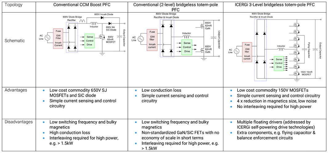
Table I: Comparison of Three Different Approaches to Low-cost High-performance PFC (Click the image to view larger size)
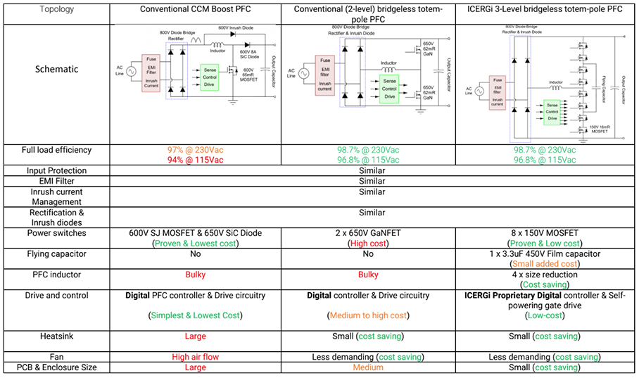
Table 2: BOM Cost and Performance Comparison (Click the image to view larger size)
Cost and Performance Comparison
Table I summarises the benefits and drawbacks of each approach as discussed. Table II compares the BOM cost and performance of the three solutions. For a fair comparison, the switching frequency is assumed to be the same and the amount of EMI noise injected back to the AC source is similar for three implementations under study.
Summary
The historical CCM boost PFC has a marginally lower cost for power switches, drive, and control as compared to that of the ICERGi PFC solution. However, if one looks at total system cost, the two solutions would be running neck and neck. The cost differences can be bridged by the benefits of the 4x inductor size reduction, smaller heatsink, smaller enclosure, less demand on fans for cooling air, and advanced digital control functionalities. Higher efficiencies also bring long-term benefits of energy-saving, e.g. lower utility bills, and the benefits of compatibility with increasing demand for green practice and standards.
The ICERGi 3-level PFC solution is easily capable of scaling-up in power. In other words, no interleaving is required for power up to 3.3kW, which would allow further system cost reduction for power above 1.5kW. The ICERGi PFC design is expected to have a lower system cost than a conventional PFC implementation with interleaving.
Moving from the conventional boost PFC to the GaN-based totem-pole PFC enables power saving with direct benefits of the smaller heatsink and less demanding cooling requirements. However, such benefits would not be great enough to compensate for the high cost of GaN devices that do not have the same economies of scale and experience curve and where single-sourced components pose a significant risk in terms of single-source component vulnerabilities.
ICERGi will present the multilevel Si power conversion technologies at APEC 2020. If you would like to talk to us, please email [email protected] or [email protected]
About the Authors
Trong Tue Vu holds a Ph.D. in Electronics Engineering, Digital Control and Implementation of Switched Mode Power Supply at Maynooth University. He also holds a Master's Degree and a Bachelor's Degree in Electrical, Electronics and Communications Engineering at Dublin City University and Ho Chi Minh City University of Technology respectively. He is currently the CEO of ICERGi Ltd. since January 2018.
Edgaras Mickus is an Electronics Engineer skilled in hardware design and programming embedded systems with 5 years of experience in R&D and is also skilled in web development which makes him well suited for bridging the gap between the two disciplines. He holds a Master's Degree in Electrical and Electronics Engineering at University College Dublin and a Bachelor's Degree in Electronic Engineering at Maynooth University. He currently works as the Lead Engineer in Digital Control at ICERGi Ltd. since August 2017.
References
-
“1kW, Compact, 97.5% Efficiency, Digital PFC for AC/DC PSUs With eMeter Reference Design”, TI Application Note, May 2016 http://www.ti.com/lit/ug/tidubk8b/tidubk8b.pdf
-
“2.2kW, High Efficiency (80+ Titanium) Bridgeless Totem-pole PFC with SiC MOSFET (TO-263-7)”, CREE Application Note, Feb 2018 https://www.wolfspeed.com/downloads/dl/file/id/1555/ product/427/crd_02ad09n_application_note.pdf
-
T. T. Vu and E. Mickus, “99% Efficiency 3-Level Bridgeless Totem-pole PFC Implementation with Low-voltage Silicon at Low Cost”, IEEE Applied Power Electron. Conf. and Expo. (APEC), Mar. 2019, pp. 2077-2083
-
G. Young, “Gate Drive Circuit for A Semiconductor Switch”, U.S. Patent 9 590 621 B2, Mar. 2017
-
T. T. Vu and G. Young, “A Method of Controlling A Current Shaping Circuit”, G.B. Patent 2549994, Jul. 2019