Facebook
 Google
 GitHub
 Linkedin
CMOS SR Latches and Flip-Flops
Learn how CMOS SR latch and flip-flop devices work.
A flip-flop is a logic circuit involving feedback – the output of a gate drives its input, primarily via other gates. Flip-flops are the basis of digital memory. The SR (set/reset) flip-flop is a basic type of flip-flops.
Combinational and Sequential Circuits
The logic output of a combinational circuit at any time depends on the logic state of the inputs at that instant of time. Hence, the output logic state is a function of the current logic state of the inputs.
In sequential circuits, the logic state of the output depends on the current logic state of the inputs and the logic state of the inputs at previous times; therefore, a new variable, the time, intervenes.
Sequential circuits can remember the previous states of the inputs and use them later to determine the output logic state.
The flip-flop is one of the essential sequential devices.
The System Clock
The system clock (Ck) is a pulse train of period T, as shown in Figure 1.
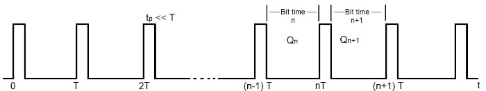
Figure 1. A clock pulse train.
The pulse width is tp. Oftentimes, the clock signal has a duty cycle of 50% meaning that the pulse width tp is half the clock period T. However, the clock waveform shown in Figure 1 has a pulse width much smaller than the clock period. As we’ll discuss below, this particular type of clock can help us create useful memory elements.
The clock signal is usually connected to several different blocks within the digital system allowing us to operate them synchronously. The transition of the binary values (logic states) in such systems occurs synchronously, i.e. they change state at a particular portion of the clock waveform.
When analyzing a sequential system, the output values corresponding to the consecutive intervals of T are usually denoted by Q1, Q2, Q3,…, Qn.
Storing 1-Bit of Information
The elementary digital gates can be interconnected to form memory elements that can be used to store the previous logic state of an input in a sequential circuit.
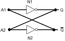
Figure 2 shows the most straightforward digital memory, cross-coupling two NOT circuits N1 and N2.
Figure 2. A 1-bit memory.
Connecting each gate’s output to the other gate’s input, we get a feedback combination commonly referred to as a latch.
A latch is a memory element characterized by having only two stable logical states at its output The circuit can remain at either state (Q = logic 1 or Q = logic 0) indefinitely acting as a one-bit memory.
The latch is a bistable circuit with two complementary outputs. Since the information is locked, or latched, in place, it is a latch.
If the output of N1 in figure 2 is Q = logic 1, the input to N2 is also logic 1. Then the output of N2 is Q̅ = 0, and the input to N1 is logic 0. Finally, the output of N1 is Q = logic 1, which matches our initial assumption.
Likewise, another possible state is Q = 0 and Q̅ =1.
The interconnection prevents having the same logic state in both outputs simultaneously.
SR Latch
We need to develop a mechanism to trigger the latch in Figure 2 and make it change state. This is achieved by the SR (set/reset) latch shown in Figure 3.
The SR latch is created by cross-coupling two NAND gates.
As we’ll discuss below, the SR latch allows us to store one bit of information.
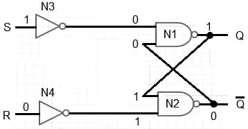
Figure 3. A set/reset latch with NAND gates.
To store a specific state, let’s say Q = logic 1 or Q̅ = logic 0 in the latch; we should apply appropriate values to the S and R inputs in Figure 3.
Figure 3 shows the state of the inputs and output when S = logic 1 and R = logic 0, which sets the latch output to the logic 1 state. The S terminal is the set, or preset, input. The latch is set when Q = logic 1 and Q̅ = logic 0.
Choosing S = logic 0 and R = logic 1 enters a logic 0 into the memory. The R terminal is the reset or clear input.
Table 1 shows the SR latch truth table.
|
S |
R |
Qn |
Qn+1 |
Comment |
|
0 |
0 |
0 |
0 |
No change of state |
|
0 |
0 |
1 |
1 |
|
|
0 |
1 |
0 |
0 |
Output = 0 |
|
0 |
1 |
1 |
0 |
|
|
1 |
0 |
0 |
1 |
Output = 1 |
|
1 |
0 |
1 |
1 |
|
|
1 |
1 |
0 |
Not allowed |
|
|
1 |
1 |
1 |
Table 1. The truth table for the SR latch.
Qn is the current state of the output at the instant of applying the input combination. Qn + 1 is the next state the output takes after applying a given combination to the inputs.
The inputs S = logic 0, R = logic 0, lead to an unknown state – Qn+1 could be either logic 1 or logic 0. With this combination of inputs, the output does not change; that is, the next state of the output is logic 0 if it was logic 0 and logic 1 if it was logic 1. In this case, the latch “remembers” its previous state.
With S = logic 0 and R = logic 1, the output goes to logic 0 regardless of whether it was in logic 0 or logic 1.
With S = logic 1 and R = logic 0, the output goes to logic 1 regardless of whether it was in logic 0 or logic 1.
The combination S = logic 1, R = logic 1 is not allowed. It produces a state of indeterminacy that must be avoided – the set and reset inputs in an SR latch cannot be logic 1 simultaneously.
Based on the above discussion, we can build table 2, which is a summary truth table.
|
S |
R |
Qn+1 |
|
0 |
0 |
Qn |
|
0 |
1 |
0 |
|
1 |
0 |
1 |
|
1 |
1 |
Not allowed |
Table 2. A summary truth table for the SR latch.
Figure 4 shows the logic symbol for a set/reset latch.
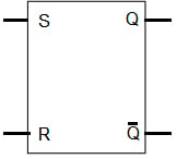
Figure 4. The logic symbol for a set/reset latch.
Figure 5 shows an SR latch achieved with NOR gates.
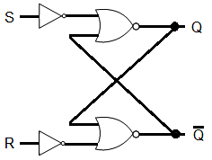
Figure 5. A set/reset latch with NOR gates.
The Clocked SR Flip-Flop
A clocked flip-flop is one improvement from the basic latch.
In order to implement sequential systems, we need to be able to set or reset the output of the memory element in synchronism with clock pulses. In the case of a clocked SR flip-flop, a clock signal similar to that shown in Figure 1 is used to set/reset the output at the appropriate moments. With a clocked SR flip-flop, the outputs change states during the brief periods of time that the clock is at logic high
Figure 6 shows a clocked SR flip-flop.
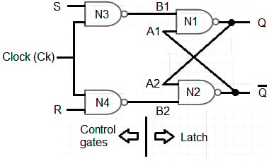
Figure 6. A clocked SR FLIP-FLOP.
The gates N1 and N2 make a latch. N3 and N4 are the steering gates to set the state of the flip-flop when the clock is at logic high.
When Ck = logic 0 (no clock pulse), the outputs of N3 and N4 are logic 1, no matter what the values of set and reset are. Under this condition, the circuit behaves like the one in figure 2 – a latch. Then, the clocked SR flip-flop does not change state within the “Bit time” intervals shown in Figure 1.
When Ck = logic 1 (clock pulse), the outputs of N3 and N4 depend on the value of the S and R inputs. If S = R = logic 0, then Qn+1 = Qn. If S = logic 0 and R = logic 1, then Qn+1 = logic 0. If S = logic 1 and R = logic 0, then Qn+1 = logic 1.
If S = R = logic 1, the outputs of N3 and N4 are logic 0. Then the N1 and N2 outputs must be logic 1. This condition is inconsistent with our definition of Q and Q̅. The output transistor of each gate N1 and N2 cut off, resulting in each output being logic 1. At the end of the pulse, the inputs at B1 and B2 rise from logic 0 to logic 1.
Depending upon which input increases faster and upon circuit parameter asymmetries, either the stable state Q = logic 1 or Q = logic 0 will result. Since the final result is undefined, we should avoid the condition S = R = logic 1.
Commercial CMOS SR Latches
Figure 7 presents a block diagram of a Fairchild CD4043BC (Quad cross-couple 3-STATE CMOS NOR latches), and table 3 shows its truth table.
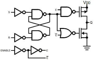
Figure 7. A Fairchild CD 4043BC.
|
S |
R |
E |
Q |
|
X |
X |
0 |
OC |
|
0 |
0 |
1 |
NC |
|
1 |
0 |
1 |
1 |
|
0 |
1 |
1 |
0 |
|
1 |
1 |
1 |
Δ |
Table 3. Truth table for the CD4043BC.
Where,
OC = Open circuit
NC = No change
X = Don’t care
∆ = Dominated by S = 1 input
Figure 8 shows a block diagram of a Fairchild CD4044BC (Quad cross-couple 3-
STATE CMOS NAND latches), and table 4 shows its truth table.
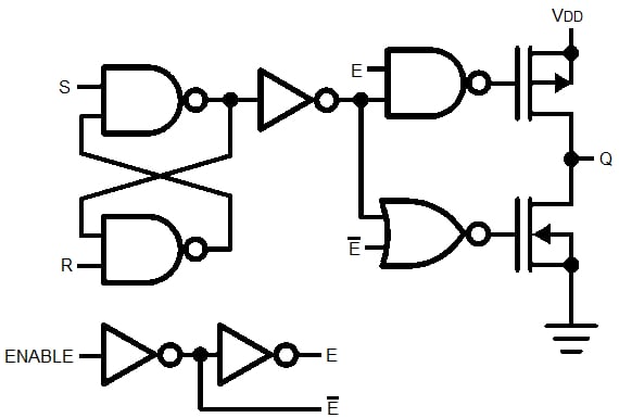
Figure 8. A Fairchild CD4044BC.
|
S |
R |
E |
Q |
|
X |
X |
0 |
OC |
|
1 |
1 |
1 |
NC |
|
0 |
1 |
1 |
1 |
|
1 |
0 |
1 |
0 |
|
0 |
0 |
1 |
ΔΔ |
Table 4. A truth table for the CD4044BC.
Where,
∆∆ = Dominated by R = 0 input
According to Fairchild’s Datasheet, “Each latch has a separate Q output and individual SET and RESET inputs. There is a common 3-STATE ENABLE input for all four latches. A logic 1 on the ENABLE input connects the latch states to the Q outputs. A logic 0 on the ENABLE input disconnects the latch states from the Q outputs resulting in an open circuit condition on the Q output. The 3-STATE feature allows common bussing of the outputs.”
About CMOS SR Latches and Flip-Flops
The present state of a combinational circuit does not depend on the previous value of the inputs – it has no memory. The output depends on the current combination of inputs only.
A sequential circuit has memory, so the output depends on the combination of present inputs and the logic state of the inputs at previous times.
A clock is an external, usually periodic logic signal, used to synchronize signals in complex circuits.
A latch can store one bit of information by remaining indeterminately in the acquired states.
The inputs to an SR latchare S (set) and R (reset). The outputs are Q and Q̅.
When the inputs R and S are logic 0, the outputs “remember” the previous states.
Making S = logic 1 – the set operation – changes the outputs to Q = logic 1 and Q̅ = logic 0.
Making R = logic 1 – the reset operation – changes the outputs to Q = logic 0 and Q̅ = logic 1.
Avoid the combination S = R = logic 1.
A clocked flip-flop accepts the input states during the brief periods of time that the clock is logic high.
Featured image used courtesy of Pixabay