Facebook
 Google
 GitHub
 Linkedin
Scientists Have Developed a Non-toxic, Visible-light Absorbing Semiconductor Material
A group of scientists from Japan recently published a study on the development of a supposedly cheaper and non-toxic narrow-gap semiconductor material with photofunctional applications.
Functional materials are applied in a wide range of technological devices like displays, communication equipment, and sensors. With increasing requirements, the development of such functional materials for micro and nano-electronic devices is an important challenge.
Many efforts have been made over the past years to develop non-toxic and cheap narrow-band materials that can absorb a wide range of UV to visible light. These functional materials contribute to the advancement in photo-function applications like solar cells, sensors, etc.
Photofunctional materials, however, are not cheap and can often be toxic. Therefore, a group of material scientists from the Tokyo Institute of Technology and Kyushu University led by Dr. Kazuhiko Maeda has developed a cheaper and non-toxic narrow-gap semiconductor material with photofunctional applications.
The scientists considered tin-containing oxide semiconductors as they are relatively inexpensive. But due to the wide optical bandgap, the material cannot absorb a wide range of visible light. The properties of a functional material can, however, be altered by changing its constituent elements. The team introduced hydride ions into the tin-containing oxide semiconductor, and by doing so, they successfully reduced the bandgap from 4eV to 2eV, making the material more photofunctional.
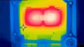
To validate the photo-functionality of the developed semiconductor material, the team tested the applicability of the material in a photoelectrode. The photoelectrode initializes the electrochemical transformation on the absorption of light. The team observed that the material gave a clear anodic photoresponse up to the expected 600nm.
Dr. Katsuro Hayashi, a professor of the Faculty of Engineering with Kyushu University says this is a big step forward in this research area.
"Overall, the study has enabled a giant leap in the development of a cheaper, non-toxic, narrow optical band gap, tin-containing semiconductor material for practical applications in solar cells, photocatalysis, and pigments,” Hayashi said.
Utilizing Narrow-gap Semiconductors
In semiconductors and insulators, electrons are confined to several energy bands and are forbidden from other areas. Bandgaps are the regions where no electronic state can exist. It is the minimum energy required to excite an electron that is in the valence band into the conduction band. The electrons — once excited and in the conduction band — are free and participate in the conduction of electricity.
In narrow-gap semiconductors, the forbidden band or bandgap is smaller than 1.11eV at room temperature. The narrow gap results in an imbalance of electron-hole population which changes the electrical property of the material. Narrow-gap semiconductors, due to their small effective masses of the electron and high electron mobility, are used in photodetectors, sensors, and high data rate communication devices. Further, the narrow bandgap enhances the performance of the photoconductive and photovoltaic devices due to their properties.
Reducing the Bandgap of the Material
The conductivity of the semiconductor materials is generally modified with the introduction of impurities into the semiconductor crystal. This process is known as doping. In this study, the team doped the hydride ions into the tin-containing oxide semiconductor and successfully decreased the bandgap from 4eV to 2eV.
The introduction of hydride ions resulted in the reduction of the tin component that accompanied the hydride ions, and led to the generation of '"tin lone electron pair" whose different electronic states notably contribute to the visible light absorption of the material. The scientists were able to accurately measure a crucial tin reduction in the material with the help of physicochemical measurements.

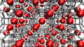
H--doped BaSn0.7Y0.3O3–δ . Image courtesy of the Tokyo Institute of Technology and American Chemical Society
For improvement in photofunctionality of the material, the scientists also give credit to the previous introduction of oxygen defects into the semiconductor material.
Dr. Maeda explains the importance of the oxygen defects in this way: "The prior introduction of oxygen defects into BaSnO3 by Y3+ substitution for Sn4+ is also indispensable to realize a significant reduction of the band gap."
A Lead-free Material
Lead is often used in piezoelectric materials, in the development of narrow-gap semiconductors, and many other functional materials. Though electronic products contain small amounts of lead, there are billions of such products used daily. Therefore, the total adds up to a very large amount of lead. Lead is a toxic heavy metal harmful to the environment. Even after recycling, a large part of e-waste (electronic waste) still ends up in a landfill.
In addition to this, an overabundance of lead can be harmful to the human body. It is absorbed into the body and displaces other chemical substances disturbing the crucial biological functions.
About the researchers
For this study, a group of materials scientists from Tokyo Institute of Technology, Nagoya University, and Kyushu University collaborated. The group was led by Dr. Kazuhiko Maeda, Associate Professor at the Department of Chemistry, Tokyo Institute of Technology. His focus areas of research include heterogeneous photocatalysis, solar energy conversion, photoelectrode, layered compounds, water splitting, hydrogen production, and CO2 reduction.