Facebook
 Google
 GitHub
 Linkedin
Keysight Debuts a GaN Test Board for its PD1500A Testing System
Advances in GaN operating voltages have made the wide bandgap technology more relevant than ever to EV manufacturers
The new Customized GaN Test Board will allow Tier 1 and OEM power converter designers employing the PD1500A to evaluate gallium nitride (GaN) semiconductors as well as silicon carbide (SiC) units

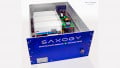
Keysight’s PD1500A. Image courtesy of Keysight
Why This Is Important
Due to their ability to operate at high frequencies, wide bandgap semiconductors (WBG) are becoming more and more widely utilized. While GaN can operate at 10MHz and SiC in the range of 100’s of kHz, so far SiC is the technology of choice in critical EV applications.
That may be about to change.
With the recent development of vertical GaN technology, it is anticipated the GaN devices will soon be able to work at 1.2kV and better, just as SiC can. Retaining its speed advantage while closing the voltage gap, GaN could soon begin to loom large in the eyes of EV manufacturers and others.
The PD1500A
The PD1500A is the star of this show, and the new test board introduced today will allow the successful device to test and characterize this new wave of ever faster, more powerful and complex semiconductor devices that are now flooding the scene.
Before the PD1500A, test and characterization systems for power devices were focused on the relatively slow silicon power MOSFETs then extant. These systems couldn’t cope with the faster edge rates and switching speeds of the fast emerging first wave of WBG power devices. This forced power semiconductor manufacturers, in conjunction with their customers, to develop custom characterization solutions.
Factors like specific gate driver designs, inductive switching and power loop parasitics will affect the dynamic parameter result.
Each analysis is valid only to a specific situation, even in the event that it is publicly available. The result is a situation where OEMs were working with very inadequate information.
The purpose of the PD1500A is to break the logjam and to provide consistent, repeatable and reliable characterizations of WBG devices. The system was initially focused on Si FETs, IGBTs, and SiC FETs. Its modular architecture minimized the need for customization of the test solution. Since introduction the PD1500A has demonstrated repeatable and reliable results for these power semiconductors.
The Challenges
GaN FETS can be an order of magnitude faster than SiC in certain uses, and the edge rates follow in proportion. Additionally, with each manufacturer optimizing their devices differently there is, as yet, little standardization.
The PD1500A is a dynamic power device analyzer and Double-Pulse Tester (DPT). To operate at GaN frequencies, the system needed to minimize power loop and gate loop inductance. Other challenges include the ability to measure a wide frequency bandwidth of parasitic currents and measuring the changing RDS(ON)s characteristic of GaN FETs
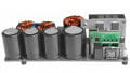
Customized Test Boards for Different GaN Device Configurations
One of the main functional capabilities of the PD1500A is its modularity. The standard PD1500A gate driver boards are easily replaced by the customized GaN test board.

The Customized GaN test board attaches to the PD1500A DPT fixture. Image courtesy of Keysight
Placing all the GaN DPT components on a single board allows for much smaller loop areas, which much smaller unwanted inductances, which enables better GaN device testing.