Facebook
 Google
 GitHub
 Linkedin
The Evolution of Application Samples
A brief history of how pre-made power electronics assemblies were created to reduce development times for utility-scale solar inverters.
The Solar Boom
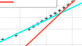
While some utility-scale solar projects already existed at the turn of the 21st century, the three years leading up to 2012 saw annual solar installations increase from 58 MW to 1.8 GW, a 30-fold increase (Figure 1). Annual utility-scale solar installations then grew to almost 80 GW in 2021 according to the International Energy Agency. Such large, decentralized energy sources pushing power to electrical grids caused increasing concerns about grid stability, as power generation became dependent on the day/night cycle as well as on weather. With electricity being an essential utility for most people, there was pressure to reduce overall costs ($/W) and the task fell upon inverter designers to simultaneously reduce system costs and increase power at the same time.

Figure 1. Historical global solar installations by year. Image used courtesy of Bodo’s Power Systems
These requirements resulted in a number of technical trends in power converters, including:
- Decreasing filter size (while meeting new power quality requirements)
- Increased DC voltage capability (e.g. 1500VDC)
- Improved grid support (e.g. reactive power, Low Voltage Ride Through (LVRT) capability)
- Better integration into energy storage systems (bidirectional operation)
These technical trends were often best served by different converter topologies that were more complex to develop. SEMIKRON created power modules to address these topologies but also had to create “Application Boards” to help connect standard driver cores to gate the devices and provide insights into how error handling was done with more complicated switching patterns. Schematics, board layouts, and Technical Explanation documents were provided to the customer to give them a head start on a production design.
These Application Boards inevitably led to the development of full “Application Samples” where module, Application Board, driver, heatsink, DC link, etc. were integrated into a working power stage. These Application Samples expanded the principle of providing customers with working power circuits where critical connections (e.g. commutation loops) had already been designed and tested.
The Shift to 3-Level with MiniSKiiP 3L Application Sample
In order to maintain the quality of the electrical grid, regulations such as IEEE 519 set maximum individual harmonics to 3% and total harmonic distortion to 5%. Grid-tie filters with inductors and capacitors smooth the output currents into a sinusoidal waveform and are required to keep solar inverters under the maximum harmonic allowance. Increasing the switching frequency of the grid-tie inverter reduces the size of grid filters as well as the material costs. However, the switching frequency is limited by losses generated in the transistors during each turn-on and turn-off operation. Three-level topologies can assist with this by almost doubling the frequency of the ripple required to be filtered over 2-level converters. Given the additional costs for more chips and driver components, a balance is needed to reduce overall system costs. Figure 2 shows some typical 3-level topologies, such as:
- NPC: Neutral Point Clamp
- TNPC: T-Type Neutral Clamp
- ANPC: Active Neutral Point Clamp

Figure 2. Typical 3-level topologies. Image used courtesy of Bodo’s Power Systems
Though many power electronics developers were experienced in 2-level voltage source inverters, such as motor drives, very few had experience with 3-level topologies. This led SEMIKRON to develop the first Application Sample, based on MiniSKiiP using NPC topology. The evaluation system supports 3-level software development while protecting the hardware, giving safety to users while developing code. A Complex Programmable Logic Device (CPLD) included in each phase leg supervises the switching sequences of the IGBTs, the dead times and the PWM sequences. The PWM signals from the control interface are routed through the CPLDs, where they are compared to a table of switching states (see Figure 3). If the PWM pattern is in the area marked green in Figure 3 (allowed switching states), the gating signals will be allowed through to the driver output stages. Destructive states, however, cause a direct connection between at least two of the three DC connections, causing current shoot-through which damages the transistors. In a potentially destructive state, the outer transistor is on and the inner transistor is off, prohibiting current due to inductance to discharge and potentially damaging the transistor from overvoltage. If the PWM pattern causes a destructive or potentially destructive state, the CPLD will shut down the phase leg using the correct switch-off sequence.

Figure 3. Safe, destructive and potentially destructive switching patterns for NPC topology. Image used courtesy of Bodo’s Power Systems
Additionally, the CPLD compares the measured analog signals with the maximum permissible values for current, temperature and voltage. If any of these exceed the safe operating range, the CPLD shuts the phase-leg down. It then ensures the inner switches (T2, T3) of the NPC topology are on before the outer switches (T1, T4) and the outer switches are off before the inner switches. Once the phase leg is back in the safe operating area, the CPLD allows operation to resume.
Increased Power at 1500VDC
In larger installations, increasing current to increase output power became prohibitive due to cable losses (I²R) and material costs, so increasing the voltage became the goal. In order to avoid the cost and safety implications of moving to a medium-voltage class, the panel voltages were increased within the limits of the Low Voltage Directive (LVD). In the early stages of solar, the limit for what was considered “low” voltage differed between Europe (1500VDC) and the USA (1000VDC), but has now been harmonized at 1500VDC.
SEMIKRON developed multiple Application Samples to test the benefits of various 3-level topologies to determine a realistic approach. The NPC topology, for example, allows switches to operate at half of the DC voltage but has a long commutation path with increased stray inductance, thereby increasing the potential for voltage spikes and affecting switching behavior. The TNPC topology, on the other hand, has a relatively short commutation path but requires devices with higher semiconductor blocking voltage, which increases switching losses.
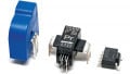
Thanks to its wide portfolio and flexibility, numerous Application Samples were based on SEMiX 5 power modules. While the early SEMiX 5 Applications Samples used the SKYPER 42 LJ driver core, this later served as a testing platform for the SKYPER 12 PV, developed specifically for 3-level solar operating up to 1500VDC and in the range of 160kVA. Two SKYPER 12 PV driver cores could fit onto a single SEMiX 5, each able to drive two IGBTs, connected via the blue Application Sample board shown in Figure 4. The blue boards actually became a designator indicating they had not gone through the rigorous SEMIKRON qualification process. Driver cores, on the other hand, are a fully qualified catalog product from SEMIKRON, indicated by the green color of the PCB.

Figure 4. Single-phase of SEMiX 5 3-Level Application Sample with two SKYPER 12 PV driver cores. Image used courtesy of Bodo’s Power Systems
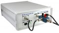
As 1500VDC utility-scale solar became dominant and inverter power was increasing, there was the need to scale up the NPC topology. SEMIKRON developed the SEMITRANS 10 Split NPC, which combined two power modules for each single phase-leg, each with a half-bridge circuit and one neutral point clamp diode. Originally based on IGBT E4, the SEMITRANS 10 contains 1200V devices, providing plenty of room at 1500VDC for overshoot and mitigating concerns about cosmic ray failure. In order to provide a simple method for customers to adapt the SKYPER 42 LJ PV driver cores to the high-power modules, SEMIKRON developed a new Application Sample capable of 1.2MW with air-cooling, as shown in Figure 5.

Figure 5. Single phase-leg of SEMITRANS 10 MLI modules with Application Board and SKYPER 42 LJ PV. Image used courtesy of Bodo’s Power Systems
3-Level Short Circuit Protection
In order to protect an inverter during a short circuit, the transistors must turn off within a specified time period, tpsc. During a shortcircuit condition, an IGBT might see many times its nominal current rating so this abnormal current must be detected and turned off within, for example, 8 or 10µs. The Application Samples implement the short-circuit protection directly on the secondary side of the gate drive circuit, providing faster response than waiting for the error signal to be sent across an isolation barrier, processed by a primary-side controller, and having the turn-off command sent back. Compared to 2-level, this process is more complicated in 3-level topologies, not only due to the turn-off sequence but increased NPC inductance loops or smaller voltage margins.
When a short-circuit occurs, the collector current in the IGBT increases, causing the collector-emitter saturation voltage, VCE,sat to increase. The driver board can measure the VCE,sat to determine whether a short-circuit is occurring, but has to wait until the IGBT is in full on-state. In order to ensure the IGBT is fully on, the detection circuit has to wait for a pre-set “blanking time”, implemented in the Application Samples.
The fast interruption of a high current inevitably means a high di/dt, leading to a high voltage spike due to stray inductances that are always present in power circuits. Slowing down the switching of the IGBT increases IGBT turn-off time (dt). This reduces di/dt and, consequently, the voltage spike across the collector and emitter of the IGBT. However, when operating with a small voltage margin, active clamping is another method used to reduce voltage spikes.
Active clamping is used to limit the voltage due to stray inductance so that the transistors do not exceed their voltage rating. In practice, this can become quite complex. As shown in Figure 6, Transient Voltage Suppressor (TVS) diodes are placed between the collector and gate of the IGBTs. The TVS diodes must be selected so that their protection voltage is greater than the operating voltage of the IGBT, but lower than the maximum voltage rating. Proper device selection is challenging, owing to the stack-up of device tolerances. The voltage characteristics of the devices also tend to be temperature-dependent. The resistor (Rclamp in Figure 6) then limits the current charging the gate and a standard diode prevents the driver from feeding into the collector in standard operation. If the SKYPER 12 senses a clamping event, it disconnects the driver stage from the gate to prevent the gate charging effect of the active clamping and the driver from working against each other. While the SEMiX 5 Application Sample only contains two clamping circuits for the most critical IGBTs (T2, T3), the SEMITRANS 10 adaptor board provides enough space to add clamping circuits to all the IGBTs. The Application Engineering team spent numerous months in the lab working with the SEMiX 5 and SEMITRANS 10 Application Sample to fine-tune the active clamping circuits.

Figure 6. Active clamping circuit for SEMiX 5 Application Sample. Image used courtesy of Bodo’s Power Systems
With the increasing demand for energy storage, many of the companies developing solar inverters began adding energy storage converters to their portfolio. For the most part, the hardware for solar and energy storage was quite similar: a 3-phase inverter coupling a DC source (now batteries instead of solar panels) with an AC grid. This concept helped reproduce the solar market’s economy of scale for energy storage, keeping converter costs to a minimum. However, the direction of power flow in the converter would occasionally reverse as the batteries were charging. This negative power factor (cos(phi) = -1) operation meant the diodes in the converter were subjected to a higher duty cycle. For example, in the NPC topology, D5/D6 clamping diodes became the limiting factor for maximum power during battery charging.
Thanks to chip innovations, generation 7 IGBTs offered smaller chips with the same current rating, enabling both an increase in IGBT nominal current from 1200A to 1400A and increased space that could be used for larger clamping diodes. Not only was the SEMITRANS 10 updated to include M7 IGBTs and a larger diode, the Application Sample was updated as well. The power electronics engineers at SEMIKRON France then developed a fully qualified power electronic stack, SEMIKUBE MLI, based on this Application Sample to reduce development time even further (Figure 7).

Figure 7. Three-phase, air-cooled power electronic stack based on SEMITRANS 10 capable of 1.25MW. Image used courtesy of Bodo’s Power Systems
Many countries are pushing to increase the share of renewable energy rather than traditional power plants. As this occurs, the countries are updating their grid codes to further ensure its stability, often including standards for Low Voltage Ride Through (LVRT) conditions. As energy grids around the world contain 50% to 100% of renewables, they need to continue operating during a blackout or brownout. Such conditions cause grid-tie inverters to output low voltage at a near-zero power factor. In such a situation, Active Neutral Point Clamp (ANPC) topology offers clear advantages. The additional transistors enable neutral point current to be split among more devices, reducing chip temperature and losses. [1]
In order to test this theory, the Application Sample shown in Figure 8 was developed. This Application Sample forms a single phase-leg of the ANPC topology (right side of Figure 2) capable of 1.3MW by including three SEMITRANS 20 half-bridge modules with the latest M7 IGBTs. The ANPC topology offers an optimized solution for both positive and negative power factors, eliminating the need to derate power at cos(phi) = -1. This enables faster development with SEMITRANS 20, the latest power module from SEMIKRON that features an industry-standard package design for high-power applications.

Figure 8. Single phase-leg of liquid-cooled SEMITRANS 20 ANPC Application Sample, capable of 1.3MW. Image used courtesy of Bodo’s Power Systems
Conclusion
The only constant in the solar market is change. As the solar inverter market evolves, so will SEMIKRON Application Samples. The main purpose is to support customer development with internal development as an added benefit. SEMIKRON continues to develop new Application Samples each year, providing a starting point for customers and reducing their development times. Rather than simply manufacturing and selling hardware, SEMIKRON gives customers the design files to enable design flexibility and speed. A global network of application engineers also supports customers who wish to adapt Application Samples to their needs, making SEMIKRON the ultimate partner in power electronics.
This article originally appeared in Bodo’s Power Systems magazine.
Related Content