Facebook
 Google
 GitHub
 Linkedin
Testing for Shoot-Through in Half-Bridge Power Converters
This article gives insight into testing for shoot-through half-bridge power converters and the influence of parasitic coupling capacitance.
Hard switching in half-bridge configurations for power converters and inverters is a commonly used technique for efficient power conversion, in particular at higher power levels. With the increasing switching speeds made possible with Silicon Carbide (SiC) technology, the potential for a short circuit across the supply resulting in shoot-through current increases. The influence of parasitic coupling capacitance from the switch node to the gate becomes more and more critical.
Coupling capacitance can lead to high-side gate glitches resulting in unwanted turn-on conditions, with both transistors of the half-bridge conducting at the same time, causing a short circuit resulting in a high current flow. Such a shoot-through current condition can destroy the transistors. Increasing the robustness of high-power designs is a critical design criterion. It is important to make sure there are no critical glitches on the high side gate of the half-bridge, with the margins between high switching speed and shoot-through conditions constantly narrowing. Increasing precision in a successful design demands increasing precision in the measuring instruments used to assess the values of critical parameters.
To verify the risk of shoot-through events, the gate to source voltage on the high-side and low-side switch have to be measured simultaneously (in the time domain, using an oscilloscope). Glitches on the high-side gate signals may not exceed a predefined voltage level in order to prevent the corresponding transistor from accidentally being turned on. This task requires a complex trigger setup for a sequence of trigger events on the high side and the low side and very high trigger accuracy, with the trigger thresholds precisely defined. After the trigger setup is configured, the device under test is operated at different load and environmental conditions to identify critical conditions throughout the specified range of operation to investigate the risk of a shoot through.
The digital trigger has made a significant improvement in the accuracy of measurements made with oscilloscopes. In contrast to an analog trigger, there is no separate trigger path. A digital trigger is applied to exactly the same digital data in real-time, and with the same resolution and bandwidth as the displayed data; if a signal can be detected by the oscilloscope, it can also be triggered.
The advantages of digital triggers for identifying critical points for verifying shoot-through risk include
- High flexibility in setting up the complete sequence of high-side and low-side trigger conditions.
- Individual setting of the trigger hysteresis to optimize the trigger sensitivity for the respective signal.
- High trigger sensitivity at full bandwidth to capture small, unwanted glitches.
- Very low jitter values for stable triggering.
- Trigger in real-time on the acquired data as it is acquired at maximum resolution and bandwidth; no critical event is missed.
Modern oscilloscopes like the R&S RTE and R&S RTO feature advanced, easy-to-use, digital triggers as well as specifications ideal for meeting power electronic test requirements.
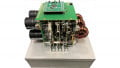
As an example of using a digital trigger, a 500 W DC/DC converter based on a symmetrical half-bridge topology is used to demonstrate how to identify critical gate timing events that can lead to a shoot through. Thanks to the real-time operation, while the trigger value for the high side gate signal is adjusted to the largest acceptable value, any switching event that violates this value, so bearing the risk of a shoot through, can be easily identified. The converter operates with input voltage between 36 V and 72 V and generates an output voltage of 3.3 V. The switching frequency is 400 kHz. According to the datasheet, the lowest possible threshold voltage of the MOSFET gate is 2 V.
After connecting the oscilloscope to the DUT, using the oscilloscope application dialog configure all relevant trigger options:
Firstly, select a trigger sequence so that it is possible to define three events (A, B, R) in a sequence. Define the first trigger event (A) as a negative edge trigger to catch the falling edge of the gate-to-sourcevoltage at the low-side switch (Figure 1). Define a suitable trigger level for this condition. This trigger event will catch every switch-off event on the low-side switching device during continuous operation of the half-bridge.

Figure 1: Trigger setup: Edge event on negative slope for trigger A at the low side switch.
Secondly, define the next trigger event (B) of the sequence to detect a glitch on the gate-to-source-terminal on the high-side switch (Figure 2). This trigger is only active after the first trigger event (A) has occurred. Define the glitch level, polarity and width values according to the worst-case condition of the application.
Thirdly, define a reset condition (R) to reset the first pre-trigger event after a specific timeout in case no glitch event has occurred. The maximum on-time of the low side switch defines the timeout value in the trigger setting.

Figure 2: Trigger setup: Glitch event for trigger B at the high-side switch.
To identify the safety margin, reduce the trigger level for the high side gate glitch trigger starting at 2 V until a trigger event happens. At 1.88 V (the green box) trigger events are generated as shown in the measurement result (Figure 3). This means a safety margin of 120 mV, in this case. The designer must decide whether this is sufficient for the robustness of the converter or inverter system.

Fig. 3: Measurement result of a half-bridge configuration
In addition to investigating the trigger, additional information about the circuit, such as the resonance frequency (in the blue box) between the leakage inductance of the transformer and the output capacitance of the switch are also determined.
About the Author
Marcus Sonst is an application engineer for Power Management at Rohde& Schwarz. He graduated in Fachhochschule Dortmund with a degree in Electrical Engineering. He was a former Development Engineer in the field of Civil and Military Aviation at Diehl Aerospace GmbH.
This article originally appeared in the Bodo’s Power Systems magazine.