Facebook
 Google
 GitHub
 Linkedin
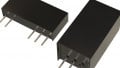
PowerBud Technology for High Current Low Insertion Force Low Resistance and Long Cycle Life Power Connectors
This article introduces the features and advantages of Methode's PowerBud, a new class of patented power connector interface, over conventional connectors
Methode has developed a new class of patented power connector interface coined as “PowerBud®”, which successfully overcomes key limitations of conventional power connectors. The PowerBud technology lowers both contact resistance and contact normal force without increasing connector volume, a capability that counters conventional wisdom. The resulting connectors exhibit lower insertion force, lower temperature rise, lower power loss and higher cycle life than conventional high current connectors.
The high current (>50A) connector design presents many design challenges. At the top of the list is the need to minimize contact resistance. Lower resistance has the beneficial effect of lowering I2R power losses, lowering contact temperature, which in turn leads to higher reliability. The lower temperature rise also allows the connector pairs to be positioned closer together in a connector housing, minimizing the connector size.
Minimizing power loss is critical for supporting the Green initiatives that work to combat adverse human impact on the earth. The energy used, which is ultimately burned up as connector heat, is wasted energy.
Low insertion force is also highly important. Insertion force is simply the mechanical force necessary to mate or un-mate the connector. Reducing insertion force has the beneficial effect of reducing contact surface wear, a major contributing cause of connector failure. With lower insertion force, collective use of multiple contacts and multiple connectors is more easily achieved. Previous efforts concentrated almost entirely on developing improved contact surface coatings and materials. Other design efforts modified the pin shape to minimize the insertion force.
This paper discusses the design tradeoffs and innovative methods to optimize current rating, contact resistance and insertion force, and how those tradeoffs led to the development of an innovative new power connector technology.
Conventional Connector Challenges
Manufacturers finely polish and plate mating contact surfaces to increase contact surface area, leading to a general misconception that current flows through the entire mated surface area. However, the actual percentage of the area that actually makes contact with the mating connector is very small.


Figure 1: Top: Surface topography showing asperities on a polished, gold-plated beryllium copper contact surface. Bottom: Contact x/z cross-sectional view taken across AU contact interface showing potential values represented as greyscale and height.
Figure 1 shows that a polished gold-plated mating surface, viewed on a microscopic level, consists of peaks and valleys called asperities. The electrical current is concentrated and passes through the asperities, which are in actual contact. The x/z cross-sectional view taken across Au contact interface shows potential values represented as greyscale and height.
The actual points of contact between mated surfaces can have a relatively high resistance and therefore a relatively high voltage drop. Each of these points of contact has a finite resistance.
One way to minimize the overall contact resistance is to have many points of contact. By placing lots of contacts “in parallel”, junction resistance is reduced.
Methods to Maintaining Low Contact Resistance
Manufacturers have adapted to the limited amount of contact area using different methods to maintain low contact resistance, including:
- Increasing the size of the mating contacts; this yields many more microscopic points of contact. The result is a larger, more costly connector.
- Increasing the “normal force” pressing the two mating surfaces together; this slightly deforms the asperities thereby increasing contact surface area. The result is a connector with high friction force that is more difficult to mate, or an expensive connector mechanism to provide the additional force after mating.
- Using a manufacturing process to reduce the surface asperities.
The need to mechanically force the mating surfaces together has led to many design compromises. Since copper is one of the very best, reasonably-priced electrical conductors (excluding gold, silver and other exotic materials), it would be a good choice for the mating parts of the connector. However, copper has poor mechanical spring properties. If both mating surfaces were pure copper, the connector would also require an additional spring to maintain copper-to-copper contact. In the connector world, that yields an expensive product.
A more practical solution is to choose a material with both spring and conductive qualities such as copper beryllium or copper-tin alloy. While less conductive than pure copper, these copper alloys are easily fabricated into a part that serves both as spring and conductor. This solution is widely used today in low-cost connectors.
Methode Develops the PowerBud® Technology
Design Engineers at Methode developed the PowerBud, a new power connector interface with superior qualities compared to conventional, commercial power connectors. The PowerBud connection interface is an evolution of power connector technology that yields an interface with exceptionally low contact resistance as well as very low insertion force without a commensurate volume increase.
PowerBud connector performance is based on maximizing the number of discrete points of contact rather than attempting to increase the contact surface area or polish the mating surfaces to a finer degree.
Furthermore, the conductors are proprietary high-performance copper alloy that is substantially better than more commonly used copper-beryllium alloys to minimize resistance. Minimal resistance allows the PowerBud technology to handle relatively large currents with very low voltage drop.


Figure 2: PowerBud mechanical construction showing two rows of contact beams having dual contact points on each beam at the interface.
The PowerBud connection interface embodies a design approach using massively parallel points of contact having a mechanical design that is adaptable to mass production. As shown in Figure 2, there are two rows of conductors arranged one over the other. The high-performance copper alloy is easily fabricated using automated processes.
A single beam conductor electrical path can be modelled as a resistor in a matrix demonstrating the cumulative parallel paths.
By arranging all individual conductors in a circular assembly results in massively parallel contact points, significantly lowering overall connector resistance. Low contact resistance means less heat generated under high current loads and less power loss.

Figure 3: New type of connector connection interface
In addition, each copper alloy conductor beam includes a slight indentation in the finger-tips to create dual contact points, adding to the massively parallel contact points. This design approach, which is illustrated in Figure 3, has yielded a new type of connector connection interface with exceptionally low contact resistance as well as very low insertion force.
MQuad vs PQ Panel Connector
The MQuad is similar to and slightly smaller than the PQ panel connector. MQuad panel connectors are also designed for blind-mate applications. As depicted in the top portion of Figure 4, each connector half floats under shoulder mounting hardware and self-aligns to the mating connector half. Contact terminations can be crimp wire, wired lugs or busbar attached. The MQuad is smaller than the PQ, and uses a 6.4mm pin rated at 100A @ 600VAC per contact with a 30ºC temperature rise.


Figure 4: MQuad connector on the top and embedded PowerBud connectors on the bottom
The embedded PowerBud connectors, as seen in the bottom portion of Figure 4, have knurled outer sidewalls allowing direct press-fit insertion into busbars, printed circuits boards and FusionLugsTM. Installation or press-in is accomplished using any flat surface and does not require any special tooling. The current rating is dependent on the physical size of the pin and the heat-sinking capability of the mounting medium.
Reducing Power Connector Package Footprint
The PowerBud is a new class of power connector offering lower voltage drop resulting in lower temperature rise and lower insertion force than competitive connectors and much less than conventional connectors.
PowerBud allows more current to pass through a connector that occupies a small volume, potentially reducing package footprint. The lower voltage drop can eliminate the need for a local voltage regulator module. The lower temperature rise reduces system thermal load.
The PowerBud is suitable for systems that require connectors capable of handling hundreds of amps of current. It is particularly suitable for systems that require the connector to be mated and unmated frequently, or systems in need of multiple connectors.
About Methode Electronics
Methode Electronics is a leading developer of custom-engineered and application-specific products and solutions utilizing the latest technologies. From magnetic signature sensing of mechanical and electrical properties to the revolutionary solid-state touch sensitive switches used in today's appliances and automobiles.