Facebook
 Google
 GitHub
 Linkedin
My Continuing Enthusiasm About 2D Material
Besides being curious and inquisitive journalists must also be enthusiastic about revolutionary new technologies. Thus, about ten years ago, I was excited
Besides being curious and inquisitive journalists must also be enthusiastic about revolutionary new technologies. Thus, about ten years ago, I was excited enough to write my first article about the promising new material “graphene” and about the hype and upheaval it would most probably trigger. But, as mostly, realization took (and takes) longer than expected.
In this case, the innovation in a way moves in horizontal direction: Materials R&D for demanding future electronics with the ability to eventually, at least partly, replace silicon point towards two-dimensional (2D) materials like graphene. In 2010, the Noble Prize made graphene famous overnight, and this gave it an additional push.
In the early days graphene produced by exfoliation was one of the most expensive materials on earth (about $100,000,000/ cm²). Meanwhile the synthesis of large-scale graphene films using chemical vapor deposition (CVD) opened the door to research on practical applications. In 2013, the European Union made a €1 billion grant to be used for research into potential graphene applications, and in the same year the Graphene Flagship consortium was formed.
Basically, graphene, made from carbon, is said to be the world’s strongest, thinnest and most conductive material. Graphene’s remarkable properties enable exciting new applications in electronics, solar panels, batteries, medicine, aerospace, 3D printing and more. There are already numerous publications, and IDTechEx – besides publishing extensive market surveys – organizes international tradeshows and conferences “Graphene & 2D Materials” in the USA and in Europe. However, though Europeans won the Noble Prize for their work on graphene, they are not necessarily winning on the commercial front: the Chinese might overtake them. Many indicators support this claim; e.g. Chinese entities are taking the patent landscape by storm and have now put a seemingly unbridgeable distance between themselves and the rest of the world. They feature heavily in the list of top ten patent holders, while there is a notable absence of Western companies and institutions.
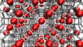
The electronic and thermal properties of graphene are tantalizing to technologists who see it as the potential basis for new kinds of electronics chips that are faster, use less power, and can flex and bend. But as it is not semi-conducting, graphene on its own lacks the characteristics necessary for transistors that are energy-efficient enough to be practical. It does not have a band gap, the electronic property that is necessary for switching transistors between two discrete states — as we all know, the development here went successfully in the direction of wide bandgap semiconductors like SiC or GaN.
Graphene´s two-dimensional – a singleatom thick – crystals combine high electrical conductivity with physical flexibility and a huge surface to weight ratio which make them highly suitable for storing electric charge in batteries and supercapacitors, and as catalysts in solar and fuel-cell electrodes. Researchers are convinced that innovative technologies will emerge from our ability to understand and control the electrochemical properties of graphene, and to fully integrate graphene with the materials used today in energy applications. Organic solar cells with better efficiency are one goal. As for batteries, commercial graphene-coated copper foils are a smart way of manufacturing novel flexible battery systems which meet mobile application requirements.
The interest in 2D materials for energy applications derives not only from their properties, but also from the possibility of cost-effectively producing and processing them in large quantities. Printable inks, for example, are the gateway to the realisation of new-generation electrodes in energy storage and conversion devices. The challenge ahead is to demonstrate a disruptive technology in which 2D materials not only replace traditional electrodes, but, more importantly, enable whole new device concepts. Swedish researchers have found a graphene-based film with four times the thermal conductivity of copper which holds a great deal of promise for the field of electronics, especially in cooling.
But 2D is not restricted to graphene. A purely theoretical mathematical study has inspired an experiment that could have serious real-world applications: a crystalline material called titanium trisulfide could perform almost as well as graphene in many areas, while lacking one key weakness. The electronic “bandgap” of titanium trisulfide is about that of silicon, potentially making it a better candidate than graphene to allow truly next-generation electronics. The computer model predicted the crystals were incredibly conductive, and had one wonderful electronic property that graphene does not: just as in silicon, the electrons orbiting within titaniumtrisulfide can be easily pushed up into the conduction band, and just as easily brought back down out of it. This means that it can be turned on and off, and in theory work as the basis for a next-generation processor. Similar layers can also be made from phosphorus. Chemists of the Munich Technical University (TUM) developed a semiconductor material (black arsenic-phosphorus, b-AsP) with highly tunable chemical compositions and electronic and optical properties. In an international cooperation with US colleagues they have built the first FETs. I hope, this will foster a successful (nonChinese) 2D R&D to keep my continuing enthusiasm alive!