Facebook
 Google
 GitHub
 Linkedin
Navitas Semiconductor Given Design Innovation Award for Power ICs
Navitas Semiconductor’s power integrated circuits (ICs) were awarded for its design innovation at the annual Shenzhen International Semiconductor and Emerging Applications Exhibition (SemiExpo).
Navitas Semiconductors is a GaN Power IC company that was founded in 2014 and has built a team of power semiconductor industry experts with a combined 200 years of experience in materials and leading-edge devices.

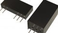
Navitas’ power devices incorporate multiple levels of design to help decrease external components while still maintaining high power density. Image used courtesy of Navitas Semiconductor.
Being ranked by performance, energy savings, and efficiency, Navitas’ gallium-nitride (GaN) power ICs, GaNFast, were selected by the China Communication Industry Association (CCIA) as the recipient for this year’s Semiconductor Design Innovation Excellence Award.
Navitas’ Award Winning GaNFast FETs
Navitas’ GaNFast technology is a wide-bandgap material that holds a lateral structure of FETs, drivers, and logic circuits rolled into a single IC. Conventional power conversion systems that derive from silicon materials are heavy, large, and inefficient over time. Navitas Semiconductor was driven to minimize system delays, eliminate parasitic inductances, cut development costs, and become a robust IC to replace silicon-based power ICs.
GaNFast FETs obtained recognition of Navitas for design innovation by CCIA thanks to its design traits. Early this month, at the SemiExpo, Navitas was amongst various manufacturers of emerging applications such as charging, AI, automatic driving, IoT, 5G communication, and intelligent sensing. Navitas ultimately was presented with this year’s design innovation award, “Navitas is honored to receive this prestigious award from CCIA and SemiExpo, recognizing the innovative achievement of GaNFast power ICs to accelerate charging in the 5G market,” said Charles (Yingjie) ZHA, VP, and GM of Navitas China.
The Impact of GaNFast FETs
Mobile device batteries are strained with rising demands for lightweight, efficient, fast charging, and longer battery life solutions for the newest technology. Integrating GaNFast power ICs allows for charging rates to increase to being 5x faster than silicon-based chargers. Navitas claims if mobile chargers implement GaNFast ICs, they will be able to charge a battery from 0 to 50% in 15 minutes.

In the graph above, it is clear that with higher frequency, silicon-based power devices fall short of GaNFast power ICs since they are optimized for high frequency, soft-switching topologies. Image used courtesy of Navitas Semiconductor.
Data Centers will always require large amounts of data being trafficked through to support our digital world. During times of heavy traffic, developers and manufacturers look for power and energy-efficient power components. Navitas’ GaNFast technology is able to improve energy savings by 40% delivering a cost-effective power device.
Whether it be improving solar inverters or electric vehicles (EVs), solar energy can help fight climate change and help save consumers money on utility fees. Renewable energy manufacturers and designers can utilize GaNFast power ICs to boost energy savings while reducing the costs of solar inverters by 20%.

Navitas GaNFast Power ICs are provided in small packaging and are able to eliminate speed-limiting and lossy discrete drive all while shrinking PCB area. Image used courtesy of Navitas Semiconductor.
Navitas claims these power ICs will bring the manufacturer’s component count down, minimize design complexity, and encourage smaller PCB footprints. Another interesting design trait is how GaNFast ICs handle digital inputs. The ICs establish clear rise and fall edged waveforms that zero out any on-chip inductance to minimize power losses. GaNFast will be impacting many industries due to Navitas designing for logic, drives, filters, and protection to be localized in a single IC. Once more manufacturers hop on the GaN-based technology, we can be sure to see Navitas moving onward to the next innovative product.