Facebook
 Google
 GitHub
 Linkedin
Vincotech and Infineon Introduce New Packaging Options at PCIM Europe
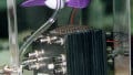
Vincotech, an independent operating unit within Mitsubishi Electric Corporation, today presented a new housing size for 90° PCB mounting called flow90 0. The first product line to be equipped with this new housing is flow90PACK 0 featuring six-pack topology. Also during PCIM Europe, Infineon Technologies AG introduced the new TO-Leadless package offering reduced package resistance, significantly smaller size as well as improved EMI behavior. It contains the latest OptiMOS MOSFETs for applications with high power and reliability requirements such as forklift, light electric vehicles, eFuse, PoL (Point of Load) and telecom systems.
Vincotech’s flow90 0 housing follows up the flow90 1 housing that Vincotech rolled out so successfully a few years ago. The idea behind this design is to mount the power module at a 90° angle to the PCB, making it so much easier to connect the module to the heat-sink in case of limited space. Where other space-saving designs require expensive L-shaped heat-sinks, flow90 0 works with standard shapes. Mounting could not be easier - it simply clips into the PCB.
The flow90 0 module's DCB with 33 x 66 mm is the same size as that of a standard Vincotech flow 0 module. With the power and chip options being the same, it can be used for much the same range of products. The choice of layouts and topologies is limited only by the special pinning concept. The housing stands 33 mm tall and is 66 mm wide, making it the perfect package for mounting several modules in book-shelf sized systems.
The first product line to feature this new housing is flow90PACK 0 comprising 1200 V modules rated from 8 to 35 A. Samples and data sheets are available on request. Serial production is slated to commence in the second half of 2013. Other topologies are available on request.
The new TO-Leadless package has been designed for high currents up to 300A. Due to its low package resistance it enables the lowest RDS(on)in all voltage classes. The 60 percent smaller package size compared to D2PAK 7-pin enables a very compact design. TO-Leadless shows a substantial reduction in footprint of 30 percent and requires less board space for example in forklift applications. The 50 percent reduced height offers a significant advantage in compact applications such as rack or blade servers. Moreover low package parasitic inductances result in an improved EMI behavior.
“With TO-Leadless Infineon is the first semiconductor company introducing a 0.75mOhm 60V MOSFET. This reduces the number of parallel MOSFETs in a forklift application and increases power density,†said Richard Kuncic, Senior Director Low Voltage Power Conversion at Infineon Technologies. “This package offers our customers significant advantages for high power applications where highest levels of efficiency and reliability are desired.â€
In addition, TO-Leadless comes with a 50 percent bigger solder contact area which leads to lower current density. This helps to avoid electro migration at high current levels and temperatures, resulting in improved reliability. Unlike other leadless packages TO-Leadless offers an optical inspection due to tin plated grooved leads. Samples of TO-Leadless are available now in 30V (IPT004N03L, 0.4 mOhms, max.), 60V (IPT007N06N, 0.75 mOhms, max.), 100V (IPT020N10N3, 2.0 mOhms, max.) and 150V (IPT059N15N3, 5.9 mOhms, max.) with production devices available in the third quarter 2013.