Facebook
 Google
 GitHub
 Linkedin
Improving Efficiency with an Active Switch on an AC Bridge
This article examines how to increase power conversion efficiency and power density with an active switch on an AC bridge.
Increasing power conversion efficiency and power density has always been the primary goal for the power supply industry. Over the past decade, there has been phenomenal progress thanks to the development of power devices, topologies, and control schemes. The evolution of super-junction MOSFETs, SiC diodes, as well as the latest GaN FETs, ensure higher switching efficiency at higher frequencies. At the same time, the implementation of advanced topologies and their corresponding control schemes is developing quickly. As a result, it is now completely feasible to achieve an optimized operating point that balances conduction loss and switching loss.
However, the diode bridge that is typically adopted as the front-end to rectify the AC line voltage remains a significant problem, impeding efficiency and power density improvement. The forward voltage drop of a high-voltage rectifier diode is typically about 1V. This means that two diodes in the main current path could lead to a total efficiency loss above 1%, especially at the low-line input.
Consider one of today’s most popular efficiency regulations, 80 Plus. 80 Plus Titanium requires 96% peak efficiency at 230VAC, and 94% peak efficiency at 115VAC. With a fairly high second-stage DC/DC efficiency at 98%, the bridge could easily consume a major portion of the budget for the PFC stage due to its high conduction loss. Moreover, the diode bridge can become the hottest spot in the power supply, which limits the power density and introduces another challenge to the thermal design.
Reducing power loss on the bridge is the next key milestone for the power supply industry. There are already solutions that address this issue, the two most popular being dual-boost bridgeless PFCs and totem-pole PFCs. Figure 1 shows that in both topologies, the rectifier diode count is reduced from two to one in the main current path, which saves conduction loss on the bridge.

Figure 1: Bridgeless PFC Topologies
Ongoing research and reference designs show promising results. However, these solutions have not been widely adopted for production by the large-volume consumer market, as there is still a ways to go toward developing a sophisticated IC solution that includes competitive BOM cost along with proven robustness and reliability. Dual-boost bridgeless PFCs require an extra, bulky power inductor to suppress the common mode noise, which is a downside from a cost and size perspective. Totem-pole PFCs usually require high-cost components such as high-side drivers and isolated current sensing. Not only that, but most of these designs are either DSP-based or are built with a large number of discrete components on a conventional PFC controller IC.
Instead of waiting for the evolution of a new controller IC with bridgeless implementations, another simple and quick alternative can instantly reduce power loss on the bridge. The basic idea is to replace the two low-side rectifier diodes with synchronous rectified MOSFETs. Meanwhile, the rest of the power supply design, including all of the power stages and the controller IC, remain the same. Figure 2 illustrates this concept using MPS’s MP6925A, a dual-channel synchronous rectifier driver that requires very few external components.

Figure 2: Bridge with Synchronous, Rectified MOSFETs on the Low-Side Bridge
The MP6925A is typically used in LLC converters. It actively drives the two MOSFETs based on the detection of the drain-source voltage (VDS). When setting up the system to replace the low-side diodes in the AC bridge, two high-voltage JFETs (QJ1 and QJ2) are used to clamp a high voltage during VDS detection. When current flows through one of the MOSFET’s body diodes, a negative threshold on VDS is triggered, and the driver turns on the corresponding MOSFET. During MOSFET conduction, the driver regulates the corresponding gate voltage to keep VDS below a certain level, until the current is too low to trigger the VDS turn-off threshold. Figure 3 shows the typical operation waveforms.

115VAC Input, Full Load

115VAC, 20% Load
Figure 3: Typical Waveforms of a Synchronous, Rectified MOSFET
A competitive synchronous rectification driver should have a very fast turn-off capability. For example, the MP6925A can turn off the gate with a delay of only 35ns when driving an equivalent 4.7nF gate capacitance. As a result, this rectifier can effectively prevent any reverse current on the MOSFET. In addition, these MOSFETs can benefit from “anti-bounce logic,” which prevents the two MOSFETs from turning on simultaneously. This leads to the whole solution being very reliable, without any risk of shoot-through.
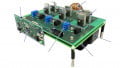
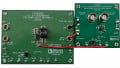
The experimental results were carried out based on a 120W adapter design, in which 650V, 99mΩ MOSFETs are used as the active switch, thus replacing two low-side bridge diodes. Figure 4 shows how efficiency is improved when the diodes have been replaced with an SR MOSFET solution. At a 115VAC low-line input, the full-load efficiency is increased by 0.43%, which means more than 0.5W is saved from the total power loss. This is a substantial improvement on both performance and thermal design for most applications.

Figure 4: Experimental Results Based on a 120W Adapter Design
An active bridge solution based on a powerful synchronous rectifier provides an instant alternative to solve issues with high power loss on the diode bridge in conventional PFCs. By replacing the bridge diodes — which have a relatively fixed forward voltage drop — with MOSFETs, conduction loss can be reduced with a lower MOSFET on-state resistance. At the same time, the power loss reduction also simplifies the thermal design. Moreover, when compared to other complex bridgeless solutions under research, this solution is based on a sophisticated IC controller with a low external component count. This makes this low-side active bridge solution a cost-effective, ready-to-use solution for practical applications.
About the Authors
Siran Wang
Siran Wang is a Technical Marketing and Application Engineering Manager at Monolithic Power Systems. He has a Ph.D. in Electrical Engineering from Zhejiang University, and he has more than 9 years working experience in the power management IC industry, with expertise in AC/DC and lighting applications.
Walter Yeh
Walter Yeh is the AC/DC team manager for Field Applications Engineers in Taiwan for Monolithic Power Systems. He has a master's degree in Electrical Engineering from National Cheng Kung University, and he has over 12 years of experience in application engineering departments for power management IC companies. His main areas of expertise are in AC/DC, lighting, and isolated DC/DC applications.