Facebook
 Google
 GitHub
 Linkedin
Improving Thermal Performance with Chip-Scale Packaged Gallium Nitride Transistors
This article discusses the advantages of chip-scale packaging of GaN transistors by evaluating its thermal performance and efficiency.
With power converters demanding higher power density, transistors must be accommodated in an ever decreasing board space. Beyond gallium nitride-based power transistors’ ability to improve electrical efficiency, they must also be more thermally efficient. In this article we will evaluate the thermal performance of chip-scale packaged enhancement-mode GaN field-effect transistors (eGaN® FETs) and compare their in-circuit electrical and thermal performance with state-of-art silicon (Si) MOSFETs.
Improving Thermal Performance
The main source of heat in a power converter generally originates from the losses inside the power transistor. Therefore, improving the thermal efficiency of the power device package is a natural starting point to improving system thermal performance. The thermal efficiency of a package can be determined by comparing two parameters, RƟJC and RƟJB, normalized to the package area. RƟJC is the thermal resistance from junction-to-case; this is the thermal resistance from the active part of the eGaN FET to the top of the silicon substrate, including the sidewalls. RƟJB is the thermal resistance from junction-to-board; this is the thermal resistance from the active part of the eGaN FET to the printed circuit board (PCB).
The junction-to-board resistance (RƟJB) of eGaN FET chip-scale packaged transistors and Si MOSFET packages generally fall on a single trend line indicating that performance for this element of thermal resistance is determined primarily by package size, and not technology [1], [2]. In contrast, figure 1 shows a plot of the thermal resistance from junction to case (RƟJC) for chip-scale packaged eGaN FETs [3], [4], represented by blue square dots, and state-of-the-art double-sided cooling Si MOSFET packages [5]-[7], represented by red circular dots. Even the most advanced double-sided cooling Si MOSFET packages are far less efficient at extracting the heat out of the top of the package than the chip-scale packaged eGaN FETs. This makes chip-scale packaging the most efficient thermal package for double-sided cooling and most suitable for high-density power designs.
![RƟJC (Junction-to-Case Thermal Resistance) for several package styles [3]-[7], eGaN FETs represented by blue square dots and Si MOSFETs represented by red circular dots](https://eepower.com/uploads/thumbnails/Efficient_Corp_Fig_1.jpg)
Figure 1: RƟJC (Junction-to-Case Thermal Resistance) for several package styles [3]-[7], eGaN FETs represented by blue square dots and Si MOSFETs represented by red circular dots
Improving Electrical Performance
The most straightforward way to improve thermal performance is to improve electrical performance, reducing power loss and therefore reducing the amount of generated heat that must be extracted. As discussed in [8], eGaN FETs have universally lower figures of merit and superior electrical packaging, resulting in improved electrical performance.
To compare the overall performance of eGaN FETs and state-of-the-art Si MOSFETs, three identical 48 VIN buck converter evaluation boards were designed, shown in figure 2. All of the boards were 2x2 inches and had active copper areas of one (1) in2 (645 mm2), outlined by the white border in the figure. The boards, designed on the same PCB panel to be consistent, had four layers of two-ounce (2.8 mils/71 µm) copper, and used an optimized layout as discussed in [8].
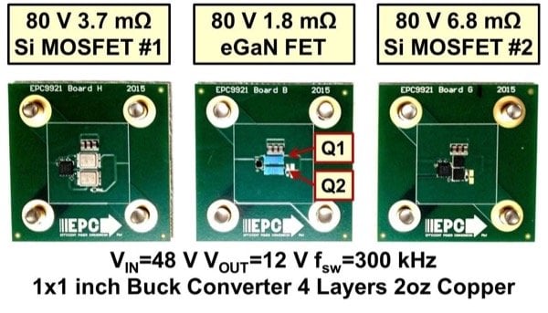
Figure 2: eGaN FET and Si MOSFET thermal evaluation boards
The 80 V Si MOSFETs used for comparison have advanced double-sided cooling packaging (Infineon BSB044N08NN3), shown on the left in figure 2, and the more traditional S3O8 packaging (Alpha and Omega Semiconductor AON7280), shown on the right in figure 2. For both Si MOSFETs, the lowest commercially available FOM devices for their respective package technologies were selected. A state-of-the-art MOSFET driver (Intersil ISL2111) was used for the MOSFET-based designs and the gate voltage for the Si MOSFETs was 10 V.
For the eGaN FET based design, shown in the center of figure 2, two 80 V Land Grid Array (LGA) chip-scale packaged EPC2021 were used with the Texas Instruments LM5113 driver and the gate voltage for the eGaN FETs was 5 V. The eGaN FET based design takes up less than half the active board area of the Si MOSFET based designs. The first reason for the improved power density of the eGaN FET-based design is that the power device is much smaller in size, when compared to the MOSFET in terms of RDS(ON) times the area. The second improvement in density is driven by the gate driver, which is also much smaller than its counterpart, in part from better packaging and in part from the reduced drive requirements of low charge, low drive voltage for eGaN FETs.
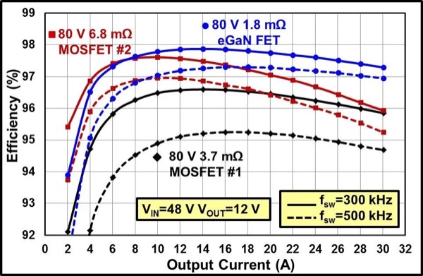
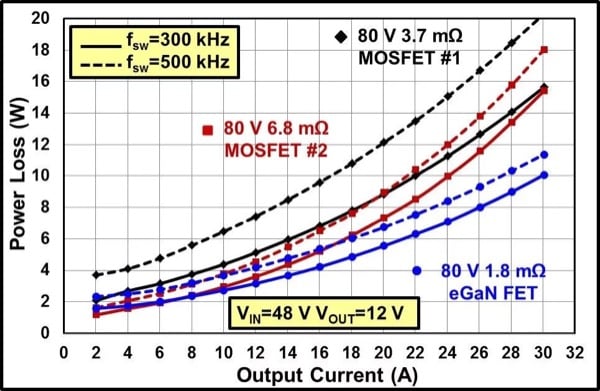
Figure 3: Experimental electrical comparison between GaN and Si-based buck converters (top) efficiency (bottom) power loss, VIN=48 V to VOUT=12 V, fsw=300 kHz and fsw=500 kHz (L=4.7 µH Coilcraft SER2915L)
The total system efficiency and power loss comparisons of the eGaN FET and silicon MOSFET based 48 VIN to 12 VOUT buck converters operated at switching frequencies of 300 kHz and 500 kHz are shown in figure 3. These plots take into account losses for the entire system, including the inductor, capacitors, and PCB losses.
The eGaN FET based design offers similar light load efficiency with the Si MOSFET #2 based design, which has an almost 4x higher on-resistance, demonstrating the effect of the low charge of eGaN FETs. At full load, the low eGaN FET on-resistance enables higher efficiency. Combining low conduction losses and low switching losses, the eGaN FET based design has higher efficiency at almost every design point.
When comparing the eGaN FET and larger Si MOSFET #1 based design, the performance is improved under all conditions. For the larger, slower switching Si MOSFET the higher switching losses become the major loss mechanism. At a switching frequency of 300 kHz and a load current of 30 A, the eGaN FET based design reduced the total system loss by 35% over both Si MOSFET based designs. At 500 kHz, the eGaN FET based design, with low switching charges, low on-resistance, and improved packaging, had a minimal drop in efficiency when compared to the Si MOSFET based designs. Furthermore, at 30 A, the total system loss is reduced by almost 40% when compared to the best Si MOSFET based solution.
Improving System Performance
In figure 4, the thermal performance of chip-scale packaged eGaN FET and Si MOSFET based designs are compared. For this work, the selected maximum temperature point for this evaluation was well below the 150°C maximum junction temperature of power devices. A 100°C maximum temperature was selected to provide margin for higher ambient temperatures and provide device de-rating, which is a common design practice.
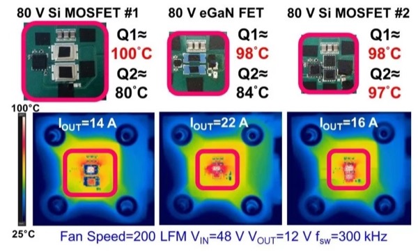
Figure 4: Experimental thermal comparison between chip-scale packaged eGaN FET (center), double-sided cooling packaged Si MOSFET #1(left), and S3O8 packaged Si MOSFET #2 (right) based buck converters without heat sinking, VIN=48 V to VOUT=12 V, fsw=300 kHz, air-flow=200 LFM, ambient temperature=25°C with same approximate maximum device temperature
At 14 A of output current, the Si MOSFET #1 based design, shown on the left of figure 4, reaches 100°C with an airflow of 200 LFM. The Si MOSFET generates higher power loss from lower electrical efficiency and the package is also less thermally efficient than the chip-scale packaged eGaN FET, shown in the center of figure 4. For the same maximum temperature, the eGaN FET based design is operated to 22 A, where the maximum device temperature matches that of the advanced double-sided cooling packaged Si MOSFET #1 on the top device (Q1). The eGaN FET based solution can achieve almost 60% more output power while maintaining the same maximum junction temperature and occupying significantly less board space.
At 16 A of output current, the S308 packaged MOSFET #2 design, shown on the right of figure 4, approaches 100°C with an airflow of 200 LFM. For the same maximum temperature, the eGaN FET based design is operated to 22 A, where the maximum device temperature matches that of the S308 packaged Si MOSFET #2 on the top device (Q1), while the low side (Q2) eGaN FET runs 13°C cooler. The eGaN FET based solution can push almost 40% more output power while maintaining the same maximum case temperature.

Figure 5: Experimental thermal comparison between chip-scale packaged eGaN FET (center), double-sided cooling packaged Si MOSFET #1(left), and S3O8 packaged Si MOSFET #2 (right) based buck converters with heat sinking, VIN=48 V to VOUT=12 V, fsw=300 kHz, air-flow=400 LFM, ambient temperature=25°C with same approximate maximum device temperature
To compare the thermal performance of eGaN FETs and Si MOSFETs capable of utilizing double-sided cooling by adding heat sinking, test cases with heat sinks were also evaluated. The heat sink and attachment methods were kept consistent between designs and followed the attachment process outlined in [1] and [2].
For the thermal evaluation with heat sinking, the chip-scale packaged eGaN FET based design, shown in the center in figure 5, reaches 100°C at an output current of 30 A with an airflow of 400 LFM. Both Si MOSFET based designs, with the double-sided cooling and conventionally packaged Si MOSFET based designs shown on the left and right of figure 5, respectively, reach 100°C at 20 A output current and 400 LFM airflow. The eGaN FET based solution achieves 50% higher overall output power, despite occupying a much smaller board space, while maintaining the same maximum case temperature. The eGaN FET shows much better junction-to-case cooling than the conventionally packaged Si MOSFET. The double-sided cooling packaged Si MOSFET occupies around three times the board area of the much smaller eGaN FET and the junction-to-case cooling improvements are similar for both designs. The eGaN FET, which is a much smaller device, has larger thermal impedance introduced by the thermal interface used to attach the heat sink. This is due to the much higher transistor density and smaller surface area to connect the heat sink.
The equivalent junction-to-ambient system thermal impedances, shown in figure 6, were calculated for the eGaN FET and Si MOSFET based designs at various airflows for the design cases with and without heat sinking. The eGaN FET based design, occupying the smallest active area, provides the best overall thermal performance. This demonstrates the chip-scale packaged eGaN FETs superior thermal efficiency when compared to even the most advanced Si MOSFET packaging methods.
When the superior thermal performance is combined with the improved electrical performance, eGaN FETs can enable improved overall system performance, in a fraction of the occupied board space. This is a combination for game-changing performance improvements.
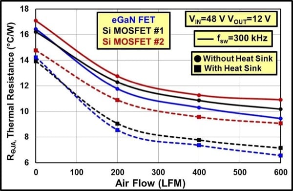
Figure 6: Comparison of junction-to-ambient system thermal impedance vs. airflow for eGaN FET and Si MOSFET based buck converters with an input voltage of 48 V, output voltage of 12 V, and switching frequency of 300 kHz
Summary
In this work, the thermal performance of chip-scale packaged GaN transistors was evaluated. For high voltage lateral GaN transistors, all of the electrical connections are located on the same side of the die, allowing for the elimination of complex, performance-limiting two-sided packaging common in vertical Si power MOSFETs. Chip-scale packaging is a more efficient form of packaging that reduces the resistance, inductance, size, thermal impedance, and cost of power transistors, enabling unmatched in-circuit performance.
About the Author
Dr. Reusch has been with the company since 2012 and is located in Blacksburg, Virginia. He received his B.S, M.S. and Ph.D. degrees in electrical engineering from Virginia Tech. While pursuing his Ph.D. degree at the Center for Power Electronics Systems (CPES) he was the recipient of the Bradley Graduate Fellowship. He has authored over 35 peer-reviewed technical publications and given numerous invited presentations related to high frequency, high-density power conversion.
Alex Lidow is CEO and co-founder of Efficient Power Conversion (EPC), former CEO of International Rectifier, and is the co-inventor of the HEXFET power MOSFET, a power transistor. He has authored numerous peer-reviewed publications on related subjects, and received the 2015 SEMI Award for North America for the commercialization of more efficient power devices. Lidow was one of the lead representatives of the Semiconductor Industry Association (SIA) for the trade negotiations that resulted in the U.S. – Japan Trade Accord of 1986 and testified to Congress on multiple occasions on behalf of the industry.
References
- D. Reusch and J. Glaser, DC-DC Converter Handbook, a Supplement to GaN Transistors for Efficient Power Conversion, First Edition, Power Conversion Publications, 2015.
- D. Reusch, J. Strydom, and A. Lidow, “Thermal Evaluation of Chip–Scale Packaged Gallium Nitride Transistors,” Applied Power Electronics Conference and Exposition (APEC), pp.587-594, 2016.
- Efficient Power Conversion EPC2001C datasheet, www.epc-co.com
- Efficient Power Conversion EPC2021 datasheet, www.epc-co.com
- Infineon CanPAK S-size BSF134N10NJ3 G datasheet, www. infineon.com
- Infineon CanPAK M-size BSB012N03LX3 G datasheet, www. infineon.com
- Texas Instruments Super SO8 Dual Cool SON 5x6mm CSD16321Q5C datasheet, www.TI.com
- A. Lidow, J. Strydom, M. de Rooij, D. Reusch, GaN Transistors for Efficient Power Conversion, Second Edition, Wiley, 2014.
This article originally appeared in the Bodo’s Power Systems magazine.
Related Content