Why You Should Use Power Stage Designer™ to Start a Power Supply Design
This article highlights Texas Instruments Power Stage Designer as a tool quick assessment values and waveforms for commonly used power-supply topologies.
Many electrical engineers have been using Texas Instruments’ free JAVA based Power Stage DesignerTM Tool since 2011 to aid them picking the right components for their switch-mode power-supplies. With the brand new version, Power Stage Designer 4.0 takes the next step in making power supply designers’ life easier. The tool now not only calculates current and voltage information for a total of 20 different topologies but also includes a very helpful toolbox, that enables the designer to start a power supply design very easily and also to finalize the power supply design more quickly.
The main purpose of Power Stage Designer is still to assist the user with calculating and visualizing general voltage and current information for the supported topologies in real-time. By clicking on the yellow highlighted components in the schematic, like in Figure 1, a window appears which displays the voltage and current waveforms for this component and some additional information like minimum and maximum voltage and current values (see Figure 2).

Figure 1: Topology window of Power Stage Designer

Figure 2: Graph window for the FET Q1 in a flyback converter displaying waveforms for voltage and current
Version 4.0 Adds Three New Topologies
Series Capacitor Buck Converter
This topology represents a special two-phase buck converter for high output current point-of-load applications, which also need a very tiny form factor. It is possible to operate this kind of converter at very high switching frequencies with reasonable efficiency levels.[1]
Quasi-resonant Flyback Converter
Low output power AC/DC converters are required to be more and more efficient. By having the flyback converter switching in a quasi-resonant mode of operation, it is possible to reduce the switching losses significantly.
LLC-Half-Bridge Converter
Inductor-inductor-capacitor (LLC) resonant topologies become more and more popular with the demands for higher power and best possible efficiency levels. With the first harmonic approximation, which is implemented in Power Stage Designer, the user can quickly assess and design the power stage of an LLC-half-bridge converter without the need to run a complex simulation. However, the design needs to be evaluated and verified afterward with simulation and a prototype.
After assessing the voltages and currents for the chosen topology, the user can now proceed with the power supply design without the need to use additional tools. The new toolbox of Power Stage Designer contains the following items to finalize the design of the power converter more quickly:
FET Losses Calculator
The FET Losses Calculator assists the design engineer with comparing and assessing the losses of different FETs. Calculations can be made for the main FET or the synchronous rectifier in a switch-mode power-supply circuit. Conductive, switching and COSS losses will be summed up for the total losses of the main FET. For the synchronous rectifier, the switching losses equal to zero due to soft-switching, but additional body diode losses contribute to the total losses. Losses due to reverse recovery effects are neglected but could become significant for very high switching frequencies. An estimation of the driver losses is also displayed.
Current Sharing Between Parallel Capacitors
Often designers do not pay much attention to the current rating of input and output capacitors in their power supply design. When different kinds of capacitors, such as ceramic and electrolytic, are used in parallel, they experienced different amounts of RMS current. If this fact is overlooked, some capacitors can experience huge stress, significantly shortening their lifetime. This tool calculates the first harmonic approximation of the RMS current for three parallel capacitors based on the impedance at the switching frequency and helps designers to choose capacitors with the appropriate current rating.
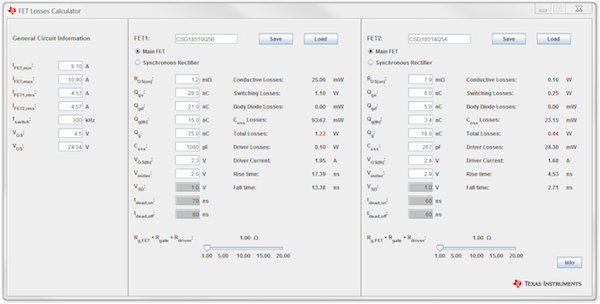
Figure 3: Power Stage Designer FET Losses Calculator window
Bulk Capacitor Calculation for AC/DC Power Supplies
AC/DC power supplies typically incorporate a bulk capacitor behind the input rectifier to provide the power stage with a quasi-constant input voltage. Power Stage Designer provides designers with a tool to quickly calculate the required bulk capacitance for their AC/DC power supply design. The recommendation depends on the minimum acceptable bulk voltage, the maximum acceptable voltage ripple, the input power, and the minimum line frequency.
RC Snubber Calculator for Rectifiers
Meeting electromagnetic interference requirements can be challenging. When the PCB layout is already final, implementing an RC-snubber network parallel to the rectifier is an option to reduce ringing in the circuit. With the RC-snubber calculator for rectifiers, designers have an easy option to get starting values for the snubber network to minimize emissions. It only requires the user to measure the ringing frequency with and without a snubber capacitor. The frequency shift caused by the capacitance gives an indication about the parasitic circuit elements, which are used to calculate the starting values for the snubber resistor and capacitor.
RCD Snubber Calculator for Flyback Converters
In flyback converters it can happen that a lot of stress is put on the FET. Especially when the PCB layout is not optimal, the board’s parasitic effects in combination with the leakage inductance of the flyback transformer can cause a huge voltage spike every time the FET is turned OFF, thus increasing the voltage level the FET needs to be able to withstand. To avoid fatal damage to the FET caused by the leftover energy stored in the leakage inductance, it is common practice to clamp the primary winding with an RCD-snubber network to the input. Power Stage Designer offers the possibility to calculate starting values for the resistance and capacitance of the RCD-snubber network.
Output voltage resistor divider
It is usually an easy task to calculate the resistor divider for setting the output voltage of a power converter. However, it can still be time-consuming to rearrange the equation from the datasheet and try different values. The output voltage resistor divider tool in Power Stage Designer lets the user select one of the feedback resistances. It then calculates the other one and the resulting output voltage. A worst case assessment is also displayed considering component and reference voltage tolerances. Effects caused by the feedback pin’s biasing current are neglected.
Dynamic analog and digital output voltage scaling
Sometimes power supplies need to have an adjustable output voltage. This can be achieved by feeding a current signal into the feedback resistor divider or by paralleling different resistors with the low-side resistor of the feedback resistor divider. Power Stage Designer offers two tools, which calculate the output voltage resistor divider plus the additional components for analog and digital output voltage scaling.
Unit Converter
Commonly used power supply parameters can be easily converted with this small tool, e.g. imperial to metric units and vice versa.
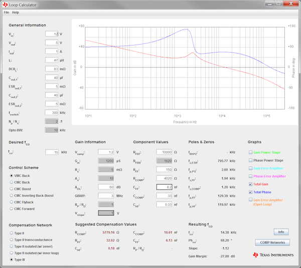
Figure 4: Power Stage Designer Loop Calculator window
Loop Calculator
The Loop Calculator tool in Power Stage Designer offers users the possibility to visualize the frequency response of different power converter topologies and their compensation networks. The graphs of the bode plot are calculated with simplified transfer functions, but will still give a good indication of how the frequency response will look like in reality. After having chosen a topology and the compensation network, the user needs to fill in some more general information about the power supply circuit and the power management controller. The effect of the chosen compensation network can be directly seen in the Bode plot of the tool. For some topologies, Power Stage Designer is able to suggest values for the compensation network based on general rules of thumb.
By the Loop Calculator supported control schemes are:
- Voltage Mode Control (VMC) Buck
- Current Mode Control (CMC) Buck
- CMC Boost
- CMC Inverting Buck-Boost
- CMC Flyback
- CMC Forward
By the Loop Calculator supported compensation networks are:
- Type II
- Type II transconductance
- Isolated Type II with Zener clamp
- Isolated Type II without Zener clamp
- Type III
Power Stage Designer is a tool that lets the user quickly assess important values and waveforms for the most commonly used power-supply topologies. The new toolbox provides additional design utilities to finalize the power-supply schematic. However, it is highly recommended to use simulation and bench testing of the prototype to verify and evaluate the power supply’s proper functionality.
The equations behind the topology calculations in Power Stage Designer can be found in the Power Topologies Handbook, the assumptions and equations behind the toolbox in the Power Stage Designer User’s Guide.
About the Author
Markus Zehendner is a Systems Applications Engineer in TI’s EMEA Power Supply Design Services Group since 2014. He holds a Bachelor in Electrical Engineering and a Master in Electrical and Microsystems Engineering from the Technical University of Applied Sciences in Regensburg. His design activity includes reference designs of isolated and non-isolated DC/DC converters with focus on automotive applications.
This article originally appeared in the Bodo’s Power Systems magazine.