Understanding the Composition of a Solar Cell
Learn about the makeup of solar cells and how they are used.
Solar radiation is converted into direct current electricity by a photovoltaic cell, which is a semiconductor device. Since the sun is generally the source of radiation, they are often called solar cells. Individual PV cells serve as the building blocks for modules, which in turn serve as the building blocks for arrays and complete PV systems (see Figure 1).
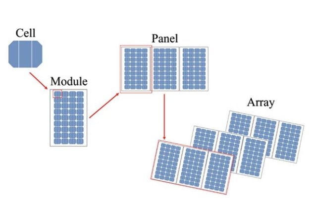
Figure 1. The basic building blocks for PV systems include cells, modules, and arrays. Image courtesy of Springer
The term "photovoltaic" is a combination of the Greek word "phos," meaning "light," and "voltage," which is named after the Italian physicist Alessandro Volta.
Semiconductor Materials
Semiconductor materials are used to make PV cells. A semiconductor is a substance that has both insulator as well as conductor characteristics. At very low temperatures, semiconductors behave as insulators, and their conductivity increases as the temperature rises. At normal temperatures, a semiconductor's electrical conductivity is between that of an insulator and a conductor. Some semiconductors also produce a voltage or exhibit a change in electrical conductivity when exposed to light.
Most PV cells utilize silicon variations altered by the doping process to make them suitable semiconductors. Doping is the process of altering the electrical properties of semiconductors by adding small amounts of impurity elements. Four valence (outer) electrons in pure crystalline silicon bond with the outer electrons of other silicon atoms to create a crystalline structure (see figure 2). When boron atoms with three valence electrons are added to silicon crystals, the boron atoms take the place of a few silicon atoms. There is an electron void in the crystalline structure where boron bonds to silicon because a fourth electron is missing. This void is also known as a hole because it can be filled by other electrons. This absence of a negative charge is referred to as a positive charge carrier. A p-type semiconductor is one that has electron voids.

Figure 2. Small amounts of other elements may be added to silicon crystals to make semiconductor materials with unique electrical properties. Image courtesy of AllAboutCircuits
When phosphorus, which has five valence electrons, is added to silicon, an extra electron is obtained at the location where the phosphorus bonds to the silicon. Since this electron is only loosely bound to the phosphorus atom, it can easily be induced to pass through the material. It is considered a negative charge carrier. An n-type semiconductor is a semiconductor that has free electrons.
The Photovoltaic Effect
The photovoltaic effect is the basic physical mechanism by which a PV cell converts light into electricity (see figure 3). When a material absorbs photons with energy above a certain threshold, the photovoltaic effect causes electrons to move within the material. A photon is a unit of electromagnetic radiation. Photons have varying amounts of energy based on their wavelength, with shorter wavelengths having higher energies. Light photons transfer their energy to electrons on the surface of a material. Extra electrons with enough energy to escape from their atoms are conducted as an electric current.

Figure 3. Free electrons are produced by the photovoltaic effect and must travel through conductors to recombine with electron voids, or "holes."
A photovoltaic cell is a p-n junction on a thin, flat wafer. A p-n junction is an intersection between adjacent layers of p-type and n-type semiconductor materials. As a p-n junction is illuminated, high-energy photons absorbed at the junction transfer their energy to electrons in the material, causing the electrons to move to a higher energy state. The electrons gain potential energy and are able to do useful work until they return to a lower energy state.

Figure 4. PV cells are wafers made of crystalline semiconductors covered with a grid of electrically conductive metal traces.
Many of the photons reaching a PV cell have energies greater than the amount needed to excite the electrons into a conductive state. The extra energy imparts heat into the crystalline structure of the cell.
When these electrons are excited, they can move around to other atoms, leaving behind voids or holes. The holes can act in a similar manner to the electrons, appearing to move when a neighboring electron moves to fill a hole, but they are associated with a positive charge. An electrical field produced by the p-n junction prevents the electrons and holes from immediately recombining, which would accomplish no work. The electrons are repelled from the p-type layer toward the cell's top surface, and the holes are repelled away from the n-type layer toward the bottom surface. This creates a difference in electrical potential (voltage) between the top and bottom surfaces.
Metal contacts on the top surface of the cell capture free electrons, while holes migrate to the bottom surface. The electrons must travel from the top surface to the bottom surface in order to recombine with the holes. This is achieved by connecting the surfaces with loads and conductors. The electrons flow through the loads, carrying out electrical work, then arrive at the cell's back surface and recombine with the holes.
This process of electrons and holes being separated by photon energy, and doing work before recombining, occurs continuously while PV cells are exposed to light. There is no way to turn off a PV device other than completely covering the surface with an opaque material so that no light reaches the cells.
Cell Materials
PV cells can be produced from a variety of semiconductor materials, though crystalline silicon is by far the most common. The base raw material for silicon cell production is at least 99.99% pure polysilicon, a product refined from quartz and silica sands. Various grades of polysilicon, ranging from semiconductor to metallurgical grades, may be used in PV cell production and affect the quality and efficiency of cells produced.
As compared to competing materials, crystalline silicon (c-Si) cells offer the best performance-to-cost ratio, and they use many of the same raw materials and processes as the semiconductor industry. However, significant research is going into developing new PV cell material technologies and also improving the performance, and decreasing the costs of existing technologies (see Figure 1).
| MATERIAL | TYPICAL COMMERCIAL SAMPLE EFFICIENCY |
BEST LABORATORY EFFICIENCY |
| Multijunction Gallium Arsenide (GaAs), concentrator | 38 to 40 | 43.5 |
| Multijunction Gallium Arsenide (GaAs), non-concentrator | 28 to 32 | 34.1 |
| Monocrystalline silicon | 15 to 18 | 27.6 |
| Polycrystalline silicon | 11.5 to 14 | 20.4 |
| Copper indium gallium selenide (CIGS) | 12 to 14 | 20.3 |
| Cadium telluride (CdTe) | 9 to 11 | 17.3 |
| Amorphous silicon (a-Si) | 8 to 9 | 12.5 |
| Dye-sensitized (Gratzel) | 8 to 10 | 11.8 |
| Polymer Organic | 2 to 4 | 10.0 |
Table 1. Various PV materials and technologies produce different efficiencies.
Gallium arsenide (GaAs) cells are more efficient than c-Si cells, but the high cost and toxicity of the GaAs materials have limited their use to space applications. Gallium can also be alloyed with indium, phosphorus, and aluminum to create semiconductors that respond to different wavelengths of electromagnetic radiation. This property is utilized to make multijunction cells, producing highly efficient cells attractive for concentrating PV applications. A multijunction cell is a cell that maximizes efficiency by using layers of individual cells that each responds to different wavelengths of solar energy. The top layer captures the shortest wavelength radiation, while the longer wavelength components pass through and are absorbed by the lower layers.
Thin-film PV devices are module-based approaches to cell design. A thin-film module is a module-level PV device with its entire substrate coated in thin layers of semiconductor material using chemical vapor deposition techniques and then laser-scribed to delineate individual cells and make electrical connections between cells. Amorphous silicon (a-Si), copper indium gallium selenide (CIGS), and cadmium telluride (CdTe) are among the competing thin-film technologies today. Thin-film modules are less costly to produce and use considerably less raw material than crystalline silicon modules, but most are less efficient than crystalline silicon and may not be as durable in the field.
A photoelectrochemical cell is a cell that relies on chemical processes to produce electricity from light rather than using semiconductors. Photoelectrochemical cells include dye-sensitized (Grätzel) cells and polymer (plastic) cells and are sometimes called organic cells. Efficiencies for these cells are still low, and corrosion from water exposure is a major issue, but this technology continues to be promising.