Wide Band Gap is No Mystery
This article highlights Siemens AG GaN power semiconductors technology in the power electronics system design that work at higher switching frequencies.<
In recent years GaN power semiconductors and GaN power electronics are mentioned in the news with revolutionary comments: “High switching speed, small size, competitive cost, and high reliability give the GaN transistor the positive trajectory to broadly displace the silicon MOSFET in power conversion applications.” [1]“GaN will take over the power transistor business.” [2]“GaN delivers nearly double power density at total cost on par with silicon.” [3]
If one considers all these promising properties of GaN power semiconductors, we should think about the question: “Why there are not more products with GaN semiconductors on the market?” Of course, there are always innovation barriers which make it complicated to use novel materials and technologies like GaN in real products. And the discussions about device reliability and higher cost for new technologies will come up in every case. If we categorize the young GaN power semiconductor technology as a disruptive technology we need to solve even greater challenges which are well known as the Innovator's Dilemma.[4]
But let’s assume that these obstacles can be overcome. Then we need to answer the following question: “What are the major challenges using GaN power semiconductors?”, but in this case from the power electronics system and application view.
Power Electronics Systems
In power electronics, we have to master a wide range of different engineering disciplines like the power semiconductor itself but also the auxiliary electronic design, the control of the power circuit, the EMC management, the power inductor design and the whole mechanical and thermal design.
GaN Power Semiconductor Technology
If we bring GaN power semiconductor technology in the power electronics system design, new challenges need to be solved if we want to use the ultra-fast switching speed of over 100V/ns. Figure 1 gives an overview of the different major engineering disciplines for a power electronics system design and some of the new challenges which come up when using fast switching GaN power semiconductors.
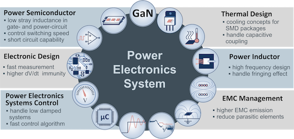
Figure 1: Engineering disciplines for the design of Power Electronics Systems
Due to the absence of reverse recovery charge and low parasitic capacitances, GaN devices switch faster and more efficient than classical power MOSFETs. Therefore the switching frequency of power converters can be increased which reduces the size of passive components such as the power inductor. From a control viewpoint, reduced inductance lowers the damping of the power circuit. This needs to be handled by the control algorithm. The classical PI-control approach often reaches its limits, therefore requiring new concepts to be developed.
Obviously, for a high transient in the switching current (> 10 A/ns) a power semiconductor package with very low parasitic inductance in the power-circuit is needed. Classical packages or modules with a parasitic inductance in a range of 10 to 20 nH will cause increased ringing and reduced switching efficiency. The high switching speed causes higher EMC emission and therefore all the electronic circuits in the system need higher dV/dt and EMC immunity. To handle the high dV/dt, parasitic capacitances should be taken into account from the beginning of the system design. It is also important to consider the thermal design and the cooling concept for SMD packages.
GaN SMD
Thermal management of a GaN SMD power semiconductor SMD (surface mount) packages enables the design of power semiconductor circuits with low parasitic inductance as well as gate drive circuits with fast and precise control of the gate voltage. Furthermore, the discrete SMD package allows easy and automated manufacturing of multilevel power converter PCBs.
On the other hand, the SMD device has a lower thermal performance in comparison to a TO-package or a power module. Since the PCB is a major part in the thermal path for an SMD power semiconductor, we have to take a closer look at the PCB design for both thermal dissipation and electrical interconnections.
Figure 2 shows a steady-state thermal equivalent circuit of a printed circuit board (PCB). Two different thermal paths of the PCB are considered: first the local thermal path under the SMD device vertical trough the PCB RPCB,v1, second the spreading resistance into the PCB RPCB,sp in combination with both a distributed vertical resistance RPCB,v2, and the convection resistance to ambient RPCB-A.

Figure 2: Thermal paths for a PCB and the steady-state equivalent circuit
PCB Thickness
All these thermal resistances can be influenced by the layout geometry as well as by different design parameters like PCB thickness, amount of copper on the surface, copper thickness of the layers, thermal VIA density and substrate material. The thermal spreading within the PCB is as important as the use of local thermal VIAs under the power semiconductor device. Thermal spreading decreases the negative influence of the thermal interface material (TIM) and board thickness.
The copper thickness of the layers is a major design parameter to improve the thermal spreading within the PCB. To analyze this influence, a simple 50x50mm2 PCB with four copper layers has been investigated. Even with a standard copper layer thickness of 70 μm or 105 μm, good thermal performance of 4K/W to 5K/W for the thermal resistance of the PCB could be reached. Furthermore, an optimized PCB design allows less local VIAs, which allows a degree of freedom for the electrical design of the power cell. This helps to design a very efficient power cell with a small loop inductance for high transients in the switching current.
The influence and the relevance of an optimized thermal PCB design are also dependent on whether the chosen cooling method is active or passive. For applications with low power losses per SMD device (approximately 4W for the mentioned above device and setup), passive cooling without a heat sink and a fan is possible. This allows for easy and cheap manufacturing of the power converter.
Passive Cooling
Furthermore, passive cooling is always an advantage for applications where a closed enclosure and long lifetime with high reliability are needed. To demonstrate this cheap and easy cooling method, a GaN converter prototype was built, which shows the feasibility of such a thermal concept. The PCB was made of standard FR4 material with 4 layers of standard 70 μm copper. The target application for this case was a three-phase bidirectional DC/AC converter with a power range of up to 5kW.
A GaN power semiconductor from Transphorm local thermal path under the SMD device vertical with 110 mΩ in a PQFN package was used. The nominal DC voltage of the design is 700 V and the line-to-line AC voltage is 400 V. The prototype was tested with a switching frequency of up to 175kHz.

Figure 3: PCB and thermal measurement of the PCB based multilevel converter at 1 kW per Phase
The pictures in Figure 3 show the design of a half-bridge of the three-phase PCB based multilevel converter. The thermal image shows the result of measurement at 1kW per phase, with 175 kHz switching frequency and an ambient temperature of 25°C. The passive cooling of the SMD power semiconductor was realized by the thermal design of the PCB. Therefore no additional heat sink or fan was used.
The Transistor T1 reaches a maximum case temperature of 57°C, which is a good value if we consider the system power and the chosen thermal concept. This value also confirms the high converter efficiency of 98,5 %, which was measured with a Yokogawa WT1800 power analyzer. For a hard switching topology, this is a good example, of the performance of the GaN technology. The board has also an LC-filter included and therefore it could generate a sinusoidal output voltage, which is shown in Figure 4.

Figure 4: Measured sinusoidal AC voltages at the output of a three-phase PCB based multilevel converter with a switching frequency of 150kHz
Outlook

Figure 5: Examples of PCB based multilevel power converter
It is well known, that GaN technology enables power semiconductors with high switching speed. GaN power electronics can work at higher switching frequencies and GaN power semiconductors in SMD packages enable PCB based multilevel converter systems with higher efficiency than comparable existing solutions. This allows the design of power converters with smaller passive components, smaller heat sinks, and higher energy density. All these advantages will lead to power electronics with a much higher level of integration (Integrated Power Electronics).
It will enable PCB based power electronics designed for an automated high volume manufacturing. On the other hand, new challenges of GaN power electronics need to be handled like: the thermal management of GaN power semiconductors; power inductors for higher switching frequencies; auxiliary electronics with higher EMC-immunity; control concepts for power circuits with a very low system damping; and concepts to handle or even to avoid the higher EMC emissions.
The increasing demand of power electronics in the growing markets for renewable energy, electromobility or factory automation could be addressed in the future with smaller, lighter and cheaper power converter systems, which are ready for an automated and high volume manufacturing.
About the Author
Marvin Tannhäuser is the head of Digital Power Electronics.
References
- Kevin J. Chen, Oliver Häberlen, Alex Lidow, Chun lin Tsai, Tetsuzo Ueda, Yasuhiro Ue-moto and Yifeng Wu; “GaN-on-Si Power Technology: Devices and Applications”, IEEE Transactions on Electron Devices, Vol.64, no.3, 2017
- Alex Lidow, “EPC: GaN Ambition”, Compound Semiconductor, July 2014, EPC: GaN Ambition
- Ahmad Bahai; “Power semiconductor technology intelligence for tomorrow’s solutions – APEC 2017”; IEEE Xplore, Ahmad Bahai Keytalk
- Clayton M. Christensen; “The Innovator’s Dilemma”, First HarperBusiness, 2000
- Robert C.N. Pilawa-Podgurski; Little Box Challenge Publication, UIUC Pilawa Group – 545-rk37Vu-57827
This article originally appeared in the Bodo’s Power Systems magazine.


