The Optimal Design for High Frequency GaN-Based Totem Pole PFC
This article highlights GaN Systems EMI filter modelling methodology for a high frequency Bridgeless Totem Pole Power Factor Correction Circuit (BTP-PFC).
GaN-based power transistors provide increased power density and efficiency in power electronics. Guidelines for selecting switching frequency and filter design are described to facilitate ease of GaN use.
It is clear that a power supply unit (PSU) running at high switching frequency with GaN HEMT devices has high power density and high efficiency. However, at a certain high frequency, attention to EMI performance of the converter is required to meet EMC regulations such as the EN55022 Class B standard. To address this objective, an analysis of an EMI filter design procedure for a Constant Current Mode Bridgeless Totem Pole Power Factor Correction circuit (CCM BTP-PFC) is presented with a result of a positive influence on the power density for high switching frequency. Additionally, the power density increase also affects efficiency, which results in a trade-off between these two quality indices. The optimal design of these tradeoffs in the BTP-PFC with GaN is evaluated in this article.
EMI Modelling and Filter Design
A typical circuit of a single-phase BTP-PFC is shown in Figure 1. To meet the EMI standard, an EMI filter is added between the topology and AC source to attenuate the noise coming from the high-speed switching behaviors of the BTP-PFC. The topology has been discussed extensively in the literature [1]. Such systems are designed for high efficiency due to neglected bridge diode loss compared to a conventional Boost PFC. The blue symbol transistors represent the high-speed leg (HS-leg) wideband gap devices (e.g. GaN HEMT). Because of the zero reverse recoveries (Qrr=0), the switching loss on the HSleg is dramatically reduced and thus can operate at hard-switching commutation with CCM which is targeting single-phase medium to high power conversion. In addition to significantly reducing switching losses, the absence of reverse-recovery behavior for the GaN HEMT is expected to result in reduced EMI generation caused by high switching di/dt, especially for radiated noise [2]. The following section focusses on the modeling methodology of conduction noise for high-frequency CCM BTP-PFC.

Figure 1: Typical BTP-PFC Circuit
As shown in Figure 2, the EMI noise is measured by a Line Impedance Stabilization Network (LISN) which is connected between the AC source and the Device Under Test (DUT). An EMI test receiver is connected to the output of the LISN in order to compare to the limits defined by the standard. This LISN actually provides a high pass filter function with the purpose of trapping the high-frequency noise current into an RC (0.1µF+50Ω) testing path. The EMI noise created by the DUT can be measured by the EMI test receiver through a 50Ω resistor. At the same time, the LISN also blocks all the noise coming from the AC source to ensure the measured noise only from the DUT. A Differential Mode (DM) EMI filter equivalent circuit of the CCM BTP-PFC is given in Figure 2 which includes two-stage LC DM filters (LDM1+CX1 and LDM2+CX2)\
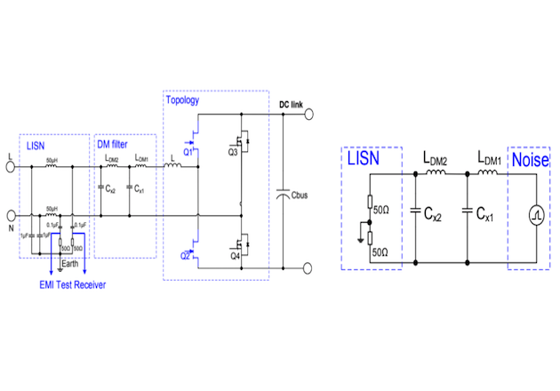
Figure 2: CCM BTP-PFC DM EMI filter equivalent circuit
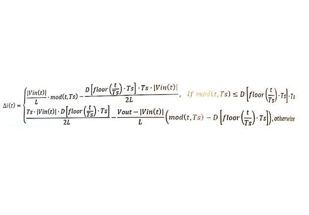
The noise is generated by the topology which has dv/dt and di/ dt switching behavior with ripple current on the PFC inductor L. In theory, for a given power rating and ripple current of inductor L, the 1st peak noise amplitude (Vnoise_pk) is determined. According to the Fourier analysis, this Vnoise_pk can be estimated by the below equation:
$$V_{noise_{-pk}} = 20log(FFT(i(t)) \cdot Zc \cdot 10^6) \ \ \ \ (1)$$
Where the input inductor current i(t) is the sum of a triangle current waveform ∆i(t) plus an AC line frequency (fline) sinusoidal shaped current:
$$i(t) = | i_{pk} \cdot sin(2 \pi f_{line} \cdot t)| + \Delta i(t) \ \ \ \ (2)$$
(3)
The ∆i(t) is the ripple current of inductor L which is calculated by equation (3) according to the inductance of L, switching period Ts, Duty cycle D, and input/output voltage Vin/Vout; Zc is the circuit impedance, for the BTP-PFC circuit, it can be represented by a resistance loading.
Based on the equations (1) through (3), the simulated DM noise spectrum is given in Figure 3 for a 1.5KW CCM BTP-PFC with 230Vac input and 400V DC output and the switching frequency of BTP-PFC are set at 65KHz and 200KHz respectively. The simulated DM noise spectrum results have the following properties:
- The noise spectrum is discrete, and the noise frequency is the integer multiplied by the switching frequency; there will be no noise between two different frequencies. When the switching frequency is at 65KHz, it is therefore below 150KHz, and the required attenuation to fulfill the EMI Class B standard is approximately 28dBµV, which occurs at the 3rd order of switching frequency, i.e. 195KHz. When switching frequency is at 200KHz, it is therefore above 150KHz, and the required attenuation to fulfill the EMI Class B standard is approximately 60dBµV, which occurs at the 1st order of switching frequency, i.e. 200KHz.
- Noise spectrum maintains -40dBµV/decade slope below the 1st noise amplitude. It can also be confirmed by the above Fourier analysis and is deduced by the previous research paper [3].
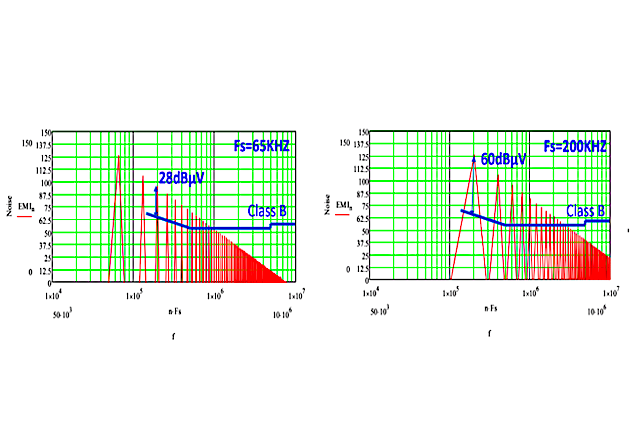
Figure 3: Simulated DM noise with frequency at 65KHz and 200KHz.
The purpose of the EMI filter is to dampen the noise above the EMI standard limitation with a sufficient design margin. As a result, the required attenuation DeltaEMI provided by the input DM filter to fulfill the EMI standard can be written as the below equation (4):
$$DeltaEMI = V_{noise_{-pk}} - V_{limit} + Margin - 40log(m) \ \ \ \ (4)$$
- Vnoise_pk is given by equation (1), which represents the 1st peak noise amplitude after 150KHz
- Vlimit is the Class B standard limit with frequency
- Margin is the EMI design margin, here we choose 6dBµV as a design margin
- m=ceil(150KHz/fs), and the function ceil represents the round-up operation, for example, if the switching frequency is 65KHz, m=3; for fs=100KHz, m=2; for fs>150KHz, m=0
- “-40log(m)” represents the noise spectrum maintaining a -40dB/ decade envelope from the 1st to nth switching frequency

Figure 4: (a) Required attenuation DeltaEMI provided by the input EMI filter (b) Two-stage LC filter insertion impedance with frequency when the DM filter’s value is 20µH+2.2µF
Based on the DM EMI noise modeling described above, we can simulate the required attenuation provided by the input EMI filter for a 1.5KW CCM BTP-PFC as shown in Figure 4(a). When the switching frequency is in the range of 50KHz to 75KHz, the worse noise frequency which is 1st noise frequency higher than 150KHZ should be the 3rd harmonic; when the switching frequency is from 75KHz to 150KHz, the worse noise frequency should be the 2nd harmonic.
There are jumping points at 75KHz and 150KHz, therefore a slight change of the switching frequency near 75KHz or 150KHz could cause a large difference in filter requirements. In other words, when choosing the switching frequency near 75KHz and 150KHz, it is recommended to set the switching frequency a little lower than the jumping point frequency. Above 150KHz, the worse noise frequency is the 1st order fundamental frequency and there will be no dramatic change on DeltaEMI after 150KHz.
After getting the required attenuation DeltaEMI, a two-stage LC filter is inserted to dampen the noise. The insertion impedance (InsertionDM) with the frequency domain is given by equation (5). Associated with the relationship between the required attenuation (DeltaEMI) and insertion impedance (InsertionDM), the values of the EMI filter can be designed at different filter corner frequencies, FC. When the absolute value of InsertionDM is equal to or larger than DeltaEMI (i.e. │InsertionDM│≥│DeltaEMI│), it can pass the EMI standard with at least 6dBµV margin.
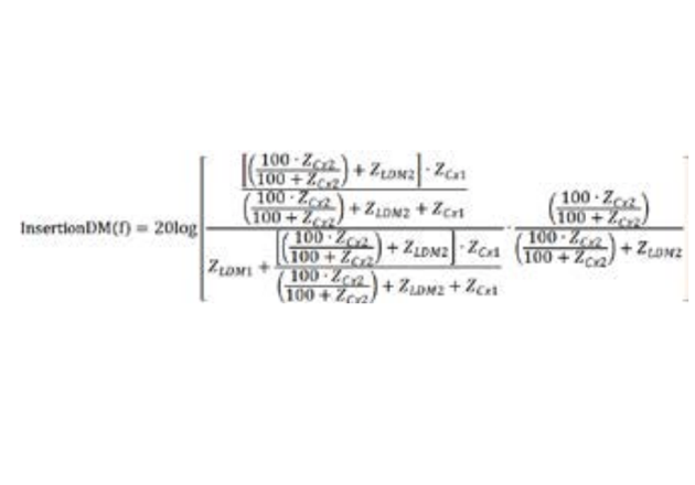
(5)
Figure 5 shows a 65KHz and 200KHz DM EMI filter design of a 1.5KW CCM BTP-PFC according to the above-derived modeling. The DeltaEMI (red line) is the required attenuation with frequency, while the blue line is the input filter frequency domain insertion impedance (InsertionDM) to dampen the noise. When the absolute value of DeltaEMI equals the absolute value of InsertionDM, the filter design can pass the EMI standard with a 6dBµV margin.
It proves with high switching frequency at 200KHz, the input EMI filter values (LDM1, LDM2, Cx1, and Cx2) are smaller with a higher filter’s corner frequency fc compared to the low switching frequency at 65KHz. As it is shown above, although the required 1st attenuation amplitude at 65KHz is lower than the one of 200KHz, the required filter’s corner frequency fc is different, meaning a higher filter’s corner frequency results to a smaller EMI filter size.
This basic modeling analysis can be applied to CM EMI filter design as well and get a similar conclusion for CM EMI design. Therefore, high switching frequency does not increase the difficulty of conduction EMI designs. On the contrary, it is helpful to reduce the size of the EMI filter and improve the power density
 Required attenuation DeltaEMI provided by the input EMI filter (b) Two-stage LC filter insertion impedance with frequency when the DM filter’s value is 20µH add 2.2µF.png)
Figure 5: 1.5KW CCM BTP-PFC EMI filter design at 65KHz and 200KHz frequencies
Inductor Dimension and Optimal Frequency
In addition to the EMI filter design, the switching frequency also impacts the BTP-PFC’s inductor design for power density. In general, the higher the switching frequency, the smaller the inductor value and size. However, with a small size, the thermal dissipation area of the inductor is limited, thus the loss and thermals of the inductor should be evaluated as a trade-off between the volume and the thermals. Fig. 6 summarizes the calculated 1.5KW CCM BTP-PFC inductor parameters with switching frequencies from 65KHz to 300KHz. The inductor’s size can be dramatically reduced from 100KHz to 200KHz with 30% volume reduction while switching frequency is up to 300KHz, the volume does not reduce much considering its temperature rise by the limitation of the thermal dissipation area

Figure 6: 1.5KW CCM BTP-PFC inductor size at different frequencies
As mentioned in the introduction, the power density increase (i.e. reduction of volume) affects the efficiency, a trade-off between these two quality indices exists. Depending on the application, the objective of efficiency and power density are weighed differently. For example, for a data center AC/DC server power supply, due to the energy savings 80+ requirement, a priority objective could be to select the target efficiency first and then improve power density as much as possible. However, for an electric vehicle on-board charger, the power density and weight matter more, and a priority objective could be to achieve a small volume and then improve the efficiency as much as possible.

Figure 7: 1.5KW CCM PFC’s peak efficiency and power density
Figure 7 shows a 1.5KW CCM PFC peak efficiency and power density relationship with switching frequency in two configurations. One is the interleaving Boost PFC with Si MOSFET and SiC Schottky diode, called Si-based PFC, and the other is the proposed BTP-PFC with GaN HEMT GS66508B used for the HS-leg, called GaN-based PFC.
For the Si-based PFC, the efficiency performance is limited by the Figure of Merit (FOM) of the Si MOSFET and additional conduction losses of bridge diodes. So, the switching frequency of Si-based PFC is normally limited below to 100KHz and a high power density is not achievable. A relatively high power density can be achieved by the use of a GaN-based PFC. According to the above EMI filter and inductor design analysis, we can calculate the GaN-based PFC’s power density improvement with respect to the switching frequency increases. It shows significant power density increase from 100KHz to 200KHz, while, above 300KHz, the power density increase is limited, and peak efficiency is below 98% due to the thermal consideration with increasing losses from the inductor and transistors.
Regarding the PFC’s efficiency comparisons, due to GaN’s benefit of low switching loss, the peak efficiency curve for GaN-based PFC remains much flatter while switching frequency is increased. Simply, GaN provides higher power density with an increased switching frequency while maintaining relatively high efficiency. For this specific 1.5KW CCM BTP-PFC design example, an optimal frequency range for GaN is 200KHz to 250KHz to trade-off the efficiency and power density.
This article describes a simple EMI filter modeling methodology for a high-frequency BTP-PFC. It concludes that GaN HEMT devices provide systems benefits of high power density with small size EMI filters and inductors while improving efficiency. An optimal frequency range for a 1.5KW CCM BTP-PFC with GaN HEMT is provided to achieve high power density and high efficiency. The data shows that GaN circuits can be designed to operate at high frequency, meet EMI requirements, and achieve high power density and high efficiency.
About the Authors
Jimmy Liu graduated electrical engineering at Huazhong University of Science and Technology and received his master's degree and Doctor of Philosophy (Ph.D.) both in the field of Power Electronics at South China University of Technology. He worked as a Technical Marketing Director at GaN Systems Incorporated Canada.
Paul Wiener received his business administration in the field of Management and Operations at U.C. Berkeley and MBA at Golden Gate University. He worked as a Vice President of Strategic Marketing at GaN Systems Incorporated Canada.
References
- GS1200BTP-EVB, “1.2kW High-efficiency GaN E-HEMT Bridgeless Totem Pole PFC Evaluation Kit”, GaN Systems Inc. (www. gansystems.com ). [2] S. Walder; X. Yuan; N. Oswald, “EMI generation characteristics of SiC diodes: Influence of reverse recovery characteristics”, 7th IET International Conference on Power Electronics, Machines and Drives (PEMD 2014). [3] B. Lu; W. Dong; S. Wang; F.C. Lee, “High-frequency investigation of single-switch CCM power factor correction converter”, 19th IEEE Applied Power Electronics Conference and Exposition, 2004. APEC '04, Volume: 3.
- S. Walder; X. Yuan; N. Oswald, “EMI generation characteristics of SiC diodes: Influence of reverse recovery characteristics”, 7th IET International Conference on Power Electronics, Machines and Drives (PEMD 2014).
- B. Lu ; W. Dong ; S. Wang; F.C. Lee, “High-frequency investigation of single-switch CCM power factor correction converter”, 19th IEEE Applied Power Electronics Conference and Exposition, 2004. APEC '04, Volume: 3.
This article originally appeared in the Bodo’s Power Systems magazine.