A High Temperature Gate Driver for Half Bridge SiC MOSFET 62mm Power Modules
This article features CISSOID CMT-TIT8243 high temperature high voltage isolated Gate Driver for 62mm SiC MOSFET power modules with High peak gate current
Today, wide bandgap semiconductors, in particular silicon carbide (SiC), are ramping up as early adopters amongst automotive OEMs are moving to this more and more mature technology offering higher efficiency and increased power density. For industrial applications, more people are also attracted by the benefits of SiC power transistors.
In order to take full advantage of fast switching and low losses SiC MOSFETs, two main challenges remain: getting well-optimized power modules featuring low parasitic inductances and having a robust and fast gate driver to reliably and efficiently drive them.
This article presents a new gate driver solution answering the key requirements of SiC MOSFET drive:
- Fast switching capability (high dV/dt) for high efficiency
- High switching frequency for high power density
- High Voltage Robustness
- Safe & Reliable Operation
Fast Switching
SiC MOSFETs allow fast switching, i.e., high dV/dt, and hence low switching losses. For a given device, switching losses can be reduced by decreasing the external gate resistors (see Figure 3). This increases the peak gate current and dV/dt. A gate driver must be able to deliver high peak gate current to enable low switching losses.
CAS300M12BM2 Module
It is worth to know that SiC MOSFET power modules are generally internally damped in order to limit the dV/dt and to avoid ringing inside the module. For example, CAS300M12BM2 module [2] has an internal gate resistor of 3 Ohms. With driving voltages of +20V/-5V, the internal gate resistor limits the peak gate current to 8.3A. It is generally recommended to add a minimum external resistance, e.g., 2.5 Ohms, to avoid any ringing.
CMT-TIT8243 Gate Driver
This means that the peak current is in practice limited to 4.5A. With a maximum peak gate current of 10A at 125°C, the CMT-TIT8243 gate driver can drive 1200V/300A SiC MOSFET modules at the maximum dV/dt and then the minimum switching losses.
Table 1: CMT-TIT8243 Gate Driver Main Characteristics
| Parameter | Conditions | Min. | Max. | Units |
| Peak gate current | Rgate_on=Rgate_off= 0Ω, Ta=125°C | 10 | A | |
| Max average gate current | Ta=125°C, V+=20V, V-=-5V | 95 | mA | |
| Positive driving voltage | -40 to 125°C, from 0 to max load | 19.4 | 20.6 | V |
| Negative driving voltage | -40 to 125°C, from 0 to max load | -5.2 | -4.8 | V |
| Parasitic capacitance | Between High-Side and Primary | 10 | pF | |
| Max dV/dt | 50 | kV/μs | ||
| Drain-Source Voltage | 1200/1700 | V | ||
| Isolation voltages | (50Hz, 1min) | 3.6 | KVrms | |
| Creepage/clearance | 14/12 | mm | ||
| Steady Operating Temperature | -40 | 125 | °C |
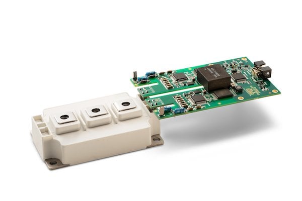
Figure 1: The CMT-TIT8243 high-temperature high voltage isolated gate driver for 62mm SiC MOSFET power modules.
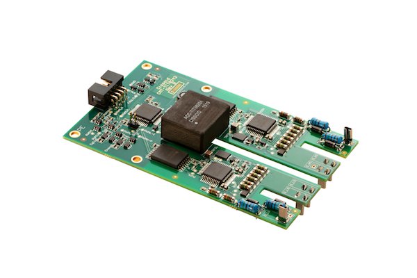
Figure 2: The CMT-TIT8243 high-temperature high voltage isolated gate driver.
Because high dV/dt is desired to reduce SiC MOSFET switching losses, designing the gate driver becomes more challenging. Indeed, high dV/dt across the parasitic capacitances of the isolation barrier, i.e., the power transformer and the signal isolators, generates a high common-mode current that can disturb the gate driver operation and can generate unwanted behavior like parasitic turn-ON or turn-OFF.
CMT-TIT8243 gate driver has been designed to provide robustness against high dV/dt: the power transformer has been optimized for low parasitic capacitance in order to minimize common-mode currents. The total parasitic capacitance is < 10pF between high-side driver and primary side, including power transformers and isolators. CMT-TIT8243 is guaranteed to operate properly at dV/dt > 50KV/μs.
![Figure 3: Switching losses versus the external gate resistance for CAS300M12BM2 module [2]](https://eepower.com/uploads/thumbnails/1917-4339-cissoid-sa.jpg)
Figure 3: Switching losses versus the external gate resistance for CAS300M12BM2 module [2]
The CMT-TIT8243 gate driver also features an RS-422 differential interface for input PWM signals to improve signal integrity during fast transitions of the power stage. With parasitic capacitances lower than 10pF between primary and secondary, with dV/dt up to 50KV/μs, common-mode currents are still close to 0.5A; this level of common-mode current could disturb inputs signals if a single-ended interface would be used. Figure 4 shows double pulse switching of the CMT-TIT8243 gate driver and CAS300M12BM2 module at 250A/600V.
![Figure 4: Double pulse switching with CMT-TIT8243 gate driver and CAS300M12BM2 module [5]](https://eepower.com/uploads/thumbnails/1917-4340-cissoid-sa.jpg)
Figure 4: Double pulse switching with CMT-TIT8243 gate driver and CAS300M12BM2 module [5]
Figure 5 shows high-side switch turn-ON with dV/dt > 40kV/μs and clean gate signals.
![Figure 5: dV/dt>40KV/μs at turn-ON with CMT-TIT8243 gate driver and CAS300M12BM2 module [5]](https://eepower.com/uploads/thumbnails/1917-4341-cissoid-sa.jpg)
Figure 5: dV/dt>40KV/μs at turn-ON with CMT-TIT8243 gate driver and CAS300M12BM2 module [5]
High Switching Frequency
Thanks to low switching losses, SiC transistors allow for an increase in the switching frequency of power converters while keeping the cooling of power devices under control. This reduces the size of filters and transformers and allows to drastically decrease the size and the weight of the power converter. To secure high-frequency switching, the isolated DC-DC converter of the gate driver must be able to supply enough average gate current, which is calculated as the total gate charge multiplied by the switching frequency.
The CMT-TIT8243 gate driver can supply an average gate current of 95mA per channel. With 1200V/300A SiC MOSFET modules having a total gate charge of about 1μC at 800V/300A [2], this means that the gate driver can operate at a switching frequency of 92KHz. In practice, the maximum switching frequency will be constrained by the switching losses in the power module rather than by the gate driver.
Achieving High Power Density
SiC MOSFET technology also helps to achieve high power density thanks to higher operating junction temperature. As the power density inside the converter increases, the ambient temperature also increases. If people are putting a lot of effort in cooling down the power modules, they often neglect the cooling of the gate driver. With an ambient operating temperature of 125°C with no derating in terms of maximum average gate current, CMT-TIT8243 gate driver offers thermal headroom for high power density converters and so eases their thermal and mechanical design.
Stable and Accurate Positive Driving Voltage
Having a stable and accurate positive driving voltage is important as the ON-resistance of SiC MOSFET decreases with the gate-to-source voltage. Dealing with important variations of the positive driving voltage implies taking larger margins in the thermal design of the power converter. CMT-TIT8243 gate driver has an accuracy better than 5% for the positive driving voltage which eases the thermal design of the power stage.
High Voltage Robustness
SiC technology brings the best benefits at blocking voltages above 600V. Also, high dV/dt and high dI/dt create voltage overshoots across the parasitic inductances inside the power loop, including the power module, the busbar and the DC bus capacitor. The gate driver is also submitted to these high voltages and must guaranty a high isolation.
CMT-TIT8243 gate driver has high isolation voltages offering safety margin in harsh voltage environments:
- Inter channel Isolation (High-Side to Low-Side) > 3600 Vrms (50Hz, 1min)
- Low-side channel isolation (Low-Side to Primary-Side) > 3600 Vrms (50Hz, 1min)
- High-side channel isolation (High-Side to Primary-Side) > 3600 Vrms (50Hz, 1min)
It has also been designed with high isolation distances for safe operation in polluted environments:
- Creepage > 14 mm (Primary to any secondary, between secondaries)
- Clearance > 12 mm (Primary to any secondary, between secondaries)
Safe & Reliable Operation
Power transistors need to be turned off with a negative voltage in order to prevent a parasitic turn-ON during the transition. However, this negative voltage needs to be well controlled as too negative gate bias can affect the long-term reliability of the gate oxide of SiC MOSFET [6]. CMT-TIT8243 gate driver has an accuracy better than 5% for the negative driving voltage.
If protections against fault is critical for gate drivers, it is even more for driving fast switching devices like SiC MOSFETs or GaN transistors. Key protections functions are:
- Undervoltage Lockout (UVLO): CMT-TIT8243 Gate Driver monitors the input primary supply voltage as well as the secondary output voltages of the isolated DC-DC converter and reports a fault when they are below the programmed threshold. Hysteresis prevents false fault event.
- Anti-overlap: this function forces a minimum non-overlapping between high- and low-side PWM signals in order to prevent turning on at the same time High-Side and Low-Side power switches.
- Active Miller Clamping (AMC): implements a bypassing of the negative gate resistor after turn-OFF to protect the power MOSFETs against parasitic turn-ON. This function is very helpful with fast-switching SiC MOSFETs generating high current through the Cgd Miller capacitance.
- Desaturation detection: at turn-ON, checks after blanking time that the power MOSFET drain-source voltage is below a threshold. If not, it likely means that a short-circuit had occurred in the power branch and the active transistor must be turned OFF. A fault must be reported to the controller.
- Soft Shut-down: in case of fault, a slow turn-OFF of the power transistor is implemented to minimize overshoots due to high dI/dt.
Conclusion
A new isolated high-voltage gated driver board optimized of 62mm SiC MOSFET power modules has been presented. Its extended temperature rating at 125°C (Ta) offers thermal headroom for the design of high-density power converters. High peak gate current enables fast switching and low losses while high average gate current support high-frequency switching. High voltage isolation and protection functions make the gate driver to safely operate in harsh electrical environments.
About the Author
Pierre Delatte is a CTO and Co-founder of CISSOID company, which the CISSOID is the leader in high-temperature semiconductor solutions, delivering standard products and custom solutions for power management, power conversion and signal conditioning in extreme temperature and harsh environments. CISSOID provides high-reliability products guaranteed from -55°C to +225°C and commonly used outside that range, from cryogenic lows to upper extremes.
References
[1] CMT-TIT8243: 1200V/1700V High Temperature (125°C) Half-Bridge SiC MOSFET Gate Driver Datasheet :
[2] P. Delatte “Designing a temperature ruggedized gate driver”, EETimes, May 2015, p40-41
[3] High-Temperature Gate Driver Primary Side IC Datasheet: DC-DC Controller & Isolated Signal Transceivers
[4] High-Temperature Gate Driver -Secondary Side IC Datasheet: Driver & Protection Functions
[5] Wolfspeed CAS300M12BM2 1200V, 4.2mOhm SiC MOSFET module datasheet
[6] R. J. Kaplar, et. al., “Degradation mechanisms and characterization techniques in SiC MOSFETs at high temperature operation”, Electrical Energy Storage Application and Technologies (EESAT) Conference, 16-19 Oct 2011, San Diego, CA, USA