DC Output for the 27 MHz Resonant Converter
This article is the third of a 3-part series describing a 27 MHz off-line converter.
This is the 3rd article in a 3 part series describing a 27 MHz off-line converter. In part one, a quasi-class E topology having ZIS turn-on and ZVS turn-off over a wide range of load impedances was described. In part two, we described power output control by tuning a load network toward or away from resonance by means of variable capacitance diodes. In this installment, we added a rectifier/filter network to convert the AC (RF) output to DC, which should have been straightforward. Instead, we encountered higher-than-expected loss in the silicon carbide Schottky diode rectifiers we tested.
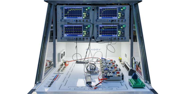
A previous design[1] was modified to obtain a DC output from the quasi-class E circuit. “AC efficiency” was first measured with a 50 volt supply and a 50-ohm load at AC_OUT. The drain waveform of Q1 was recorded.
A rectifier/filter network was then connected to the class E output. A substitution power measurement was made by loading the rectifier at DC_OUT with a variable resistor. The load was adjusted to provide the same DC input power and drain waveforms as the 50-ohm load. Equivalent power occurred with a load of 510 ohms. Measurements were made after 1 hour of continuous operation with a load current of 0.215A at 110 VDC output. AC and DC efficiency were compared.

Figure 1: Class E with DC Output.

Table 1: AC and DC Conversion Efficiency Compared
Temperature rise for both pairs of diodes was measured. For this measurement, a DC current source was substituted and adjusted to produce the same diode temperature rise as the rectification condition. A temperature rise of 79C occurred with GeneSiC (TO-220) devices. The apparent power dissipation was 1.8watts per diode or 3.6 watts total. For the Cree (D-Pak) diodes the temperature rise was 44C, indicating a power dissipation of 0.39 watts per diode or 0.78 watts total.
At 125C with 1A forward current, the GeneSiC diode data sheet[2] specifies a 2.1V typical forward voltage drop. Diode current was measured with a Tektronix P-6022 current probe. Peak forward current was 1.1 amperes.
To support a 0.215A load current the average current in each diode must be the same, i.e. 0.215 amps. Using a 2.1 volt drop and the average current of 0.215 amperes and 1.1 amperes peak, the forward dissipation of each GeneSic part should have been 0.45 Watts. The measured dissipation was 4 times greater.
The peak forward current of the Cree 1A 600V devices was 0.8 amperes. Cree specifies (at 100C) a forward voltage drop of 1.4V at 0.8 amperes. Again, the average current is 0.215 Amps. The expected dissipation of a “zero recovery” diode using the average current was expected to be 0.30 watts. The measured dissipation was 0.39 watts.

Figure 2: Varactor Effect Test Circuit.

Table 2: Measured Silicon Carbide Diode Properties.
In an attempt to gain insight into the unexpected loss, a resonant flyback circuit was modified. A 2A, 1200V SiC diode, C4D02120, was added as shown in shown in Figure 2. As bias was made more negative, diode junction capacitance decreased. C1 was increased to maintain the same peak-peak voltage across the diode. Diode dissipation decreased with increasing reverse bias (less junction capacitance, lower high-frequency current). The reverse bias diode voltage was variable over a 700 volt range.
During previous tests of the varactor effect [5], we used back to back 8A 1200V SiC diodes as varactors. In those tests, we measured 4 watts dissipation (2 watts per diode).
We tried to predict loss that might result from a 5.5-ohm internal diode resistance scenario. The rightmost column in Table 2 shows this prediction. While the reasonable agreement with actual dissipation was had at higher reverse voltages, the measured dissipation departed from our hypothesis of constant ESR at lower bias voltages. We note that our equivalent “diode resistance” was lower at -200V bias than expected, about 3 ohms.
Discussion
Our quasi-class E converter requires a high voltage power device. The ratio of peak drain voltage to DC voltage is about 3.5:1. Operation at high line (132 VAC) causes peak drain voltage in excess of of650 Volts, exceeding the maximum rating of currently available gallium nitride parts. Low-loss variable capacitance diodes in the kilovolt range are also an issue.
With present technology, the designs presented may not be suitable for off-line application in the general power supply market. A good fit for our concept might be in the fields of dielectric heating, medical diathermy, cautery applications, and near-field wireless power transfer.
A major semiconductor house is rumored to be releasing a family of low gate resistance 1700V silicon carbide MOSFETS during Q1 2019. This may be an enabling technology for world-wide off-line capability at high power, assuming device losses are reasonable.
Efficiency improvement and size reduction of any power conversion topology in the 3-30 MHz range are hampered by currently available magnetic materials. To achieve low loss at 27 MHz, both ferrite (such as 4F1) and powdered iron (such as Carbonyl E) magnetics require very low flux densities, making for bulky inductors. Solenoid or toroidally-wound air-core inductors may be the only option.
Our converter and control topology provide reasonable efficiency at higher power, although efficiency at lighter loads is less. A possible workaround might be pulse width modulation of the 27 MHz drive signal with a lower frequency, to maintain efficiency at low output power levels.
We noted previously[1] that regulatory problems may result from variable frequency control of a power supply/RF generator. FCC Part 15 requirements[4] include frequency ranges (“restricted bands”) where spurious emission limits are strict.
For wide range frequency control of converters such as the L-L-C or series resonant topologies, a frequency range of at least 2:1 is required. However, there is no 2:1 frequency range from 3 to 30 MHz that would allow variable frequency control of a converter without incursion into one or more of the FCC Part 15 restricted bands. In the (narrow) ISM frequency bands, allowable spurious emissions are greater relative to non-ISM frequencies.
We stated that it should be possible to design an L-L-C converter operating at a fixed frequency, employing electronically variable resonant power control as described in Part 2 of this series[5]. The reduction in the cost and complexity of additional shielding and filtering could be substantial.
Conclusion
In this series, we presented designs and data for a quasi-class E converter capable of operating into a wide range of inductive and resistive loads while maintaining ZIS turn on and ZVS turn off waveforms. We described two variable-reactance control methods to vary output power over a wide range.
We eliminated the need for a pre-converter, such as a buck or a boost regulator, to control output power. This offers significant cost and size reductions for certain applications.
Conversion of RF output to DC was described. We observed higher-than-expected dissipation in silicon carbide diode rectifiers. Similarly, higher than expected losses were found when reverse-biased SiC devices were used as varactor diodes.
About the Author
David Pacholok has operated Creative Electronic Consultants LLC since 1981. His interests include switch mode power conversion, electronic ballasts, RF power, pulse power, and induction heating. He can be reached at 847-809-2786 (cell), 847-428-5676, or by email at [email protected].
Paul Reich is a freelance consultant. His specialties are radio frequency design and simulation. In a previous life, he held various positions at Motorola, Inc. and the Chamberlain Group. Paul earned his BSEE in 1976.
Jim Spangler is President of Spangler Prototype, Inc. Previously, Jim was a Field Application Engineer. He is active in several IEEE societies. Jim has published extensively about power electronics applications. He can be reached at 847-961-8588 (cell) or [email protected]
References
- D. Pacholok, P. Reich, J. Spangler, “Quasi-Class E Achieves Power Control And ZIS/ZVS”, Bodos Power systems, November 2018
- N. O. Sokal et al, “High Efficiency Tuned Switching Power Amplifier”, US Patent 3919656, Nov 11, 1975
- N.O. Sokal, “Class E RF Power Amplifiers”, QEX Magazine, Jan/Feb. 2001.
- US CFR Title 47, Part 15, ppg 809 et seq.
- D. Pacholok, P. Reich, J. Spangler, “Controlling Power at 27 MHz With Variable Reactance”, Bodos Power systems, December 2018
This article originally appeared in the Bodo’s Power Systems magazine.