EPC Says its New 40 V GaN FET Is World’s Smallest at 1.1 mΩ
The fresh EPC2066 is an enhancement-mode gallium nitride (eGaN) power FET expanding the company’s extensive portfolio of low-voltage, high-current GaN transistors.
With an RDS(ON) specification 27% better than that of its footprint-compatible cousin, Efficient Power Conversion (EPC) says its latest eGAN FET, the EPC2066, is in a category of its own. No other FET in the world, the company claimed in its May 25 press release announcing this latest offering, sports an on-resistance of 1.1 mΩ in a footprint measuring just 13.9 mm2.
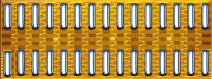
The EPC2066, in its passivated die form. Screenshot used courtesy of EPC
Still, the EPC2066 is not without company.
The device has been designed to complement the EPC2071, which EPC introduced early last month and claims is also the smallest GaN FET for its given voltage and on-resistance ratings. Together, the two form the heart of the company’s EPC9174 reference design and evaluation board for a 1.2 kW, 48 VDC to 12 VDC power converter. The EPC2071 is featured on the primary side, while the EPC2066 serves on the secondary.
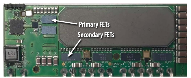
The EPC9174 demo board. Screenshot used courtesy of EPC
Both products target high-density DC-DC conversion in applications such as servers and artificial intelligence. Each is also well-suited, EPC says, to high-density BLDC motor drive applications, with the EPC2066 purposed to a range between 24 and 32 V.
The EPC2066 and EPC2071 — Specifications
Both GaN FETs are offered exclusively in passivated die form, as illustrated in the image above. Die size for the EPC2066 is 6.05 x 2.3 mm, while the corresponding figure for the EPC2071 is 4.45 x 2.3 mm. These FETs operate over a -40 to +150 ℃ temperature range, and are halogen-free and RoHS-compliant.
The EPC2071 features a maximum voltage of 100 V, a maximum continuous current of 64 A, and an on-resistance of 2 mΩ.
The EPC2066 and the EPC2071, in that order, sport these other important typical dynamic characteristics:
- Total gate charge (Qg): 25 nC, 18 nC
- Gate-to-drain charge (Qgd): 3.2 nC, 1.8 nC
- Output charge (Qoss): 59 nC, 71 nC
Both GaN FETs feature zero source-drain recovery charge (Qrr).
Why is RDS(ON) So Vital?
AC power can be fed into a transformer to raise or lower its voltage level. This isn’t possible with DC, because transformers don’t respond to steady power.
Power transistors of all sorts are designed to turn ON and OFF thousands of times a second, generating pulsating DC that behaves in a manner similar to AC, in that its voltage can be raised or lowered by the transformer. The trick is to lose only the absolute minimum power across the transistor, which acts basically as a super-fast, non-mechanical switch.
RDS(ON) is the resistance (R) between the transistor’s drain (D) and source (S) pins when the “switch” turns ON. It is the drain-to-source (d-s) pathway that is the conduit through which the switch conducts.
Because power is equal to current squared times voltage (I2R), a given current will waste more power across a device with a higher RDS(ON) than it will for a device whose on-resistance is lower.
What are Wide Bandgap Semiconductors?
GaN semiconductors are one type of wide bandgap semiconductor, the other being silicon carbide (SiC).
A wide bandgap means that it takes more energy to move an electron up to the conduction band. This has many implications for semiconductor designers, including higher operating voltages and temperatures as well as higher switching speeds.
Those higher switching speeds are particularly noteworthy, because if employed in a power supply or voltage converter, they enable filtering components to be significantly smaller, saving space and weight.
The Reference Design
The EPC9174 is an LLC Converter, a 1.2 kW module that accepts a 40-to-60 V input and delivers 12 V at 100 A. It is sized at 22.9 by 58.4 mm (1/8 brick).
As do similar topologies, the reference design features an input and output side, electrically isolated from each other but in constant communication. This allows an “informed” primary side to energize the secondary side at just the right point in the secondary side’s AC cycle. By doing this, the designer can optimize characteristics such as efficiency, EMI and/or power factor.
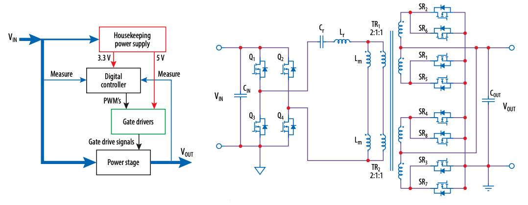
A simplified schematic of the EPC9174 LLC module. Image [modified] used courtesy of EPC
Designing these sorts of converters is highly complex, and calls for very specialized electrical engineering. The EPC9174 is not designed as a finished product, but rather as a guide to make the task easier for OEM customers.