Applied Power Electronics Conference and Exposition APEC 2017
This article discusses the 2017 Applied Power Electronics Conference and Exhibition that was held at the Tampa Convention Center, Tampa, Florida.
The 2017 Applied Power Electronics Conference and Exhibition (APEC-2017) was held from March 26-March 30 at the Tampa Convention Center, Tampa, Florida, USA. The conference, which is jointly sponsored by the IEEE Power Electronics Society (PELS), the IEEE Industry Applications Society (IAS) and the Power Sources Manufacturers Association (PSMA) brings together professionals from all sectors of the power electronics industry for in-depth technical presentations and discussions that combine theory with practical applications.
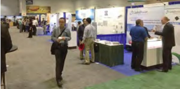
Attendees stroll the exhibit hall at APEC 2017
This year’s technical program was organized into technical sessions, industry sessions, exhibitor seminars and an evening of rap sessions. Over 500 papers were presented covering all aspects of applied power electronics. The papers for the technical sessions were chosen through a rigorous peer-review process to ensure high-quality presentations. For the industry sessions, the speakers were invited to make a presentation only, without submitting a formal manuscript for the APEC Proceedings. This allows for information on current topics that would not otherwise be publically presented at a professional conference. While many of these are technically oriented, some also address business-related issues. The exhibitor seminars were a series of half-hour presentations that provided a more in-depth discussion of exhibitor’s products and services than could be obtained by a visit to their booth.
A series of Professional Education Seminars were held prior to the start of the technical program. The Professional Education Seminars address the need for an in-depth discussion of important and complex power electronics topics. Each seminar combined practical applications with theory designed to further educate the working professional in power electronics and related fields. The Professional Education Seminars at APEC are three and one-half hours (including breaks) in length, range from broad to narrow in scope, and can vary from introductory to advanced in technical level. The 18 seminars covered a wide range of topics including design, control, EMI and reliability, components and systems, SiC devices, and wireless charging and magnetics.
In addition to the technical sessions, 269 exhibitors were on hand to provide attendees the opportunity to examine product offerings, design tools, and services from the leading suppliers in the power electronics industry. The conference also offered numerous opportunities for professional networking, including an Exhibit Hall Welcome Reception and a social event themed “Little Havana” featuring food, entertainment, games, and antique automobiles.
Wide-bandgap materials and devices were once again a major focus of the conference program as numerous presentations discussed the commercialization of both GaN and SiC devices. Significant attention was devoted to the reliability and robustness of these devices in applications such as electric and hybrid electric vehicles, industrial power converters, and consumer applications.
A plenary presentation by L. Stevanovic described General Electric’s approach to developing a silicon carbide-based MW-scale converter. The 2.5 MW utility-scale converter uses a new generation of high-performance SiC MOSFETs with voltage rating from 1.2-3.3 kV and current ratings up to 100A per die. Extensive stress testing was described that verified device safe operating area, avalanche capability, short-circuit ruggedness, and body diode surge capability.
A number of presentations from Wolfspeed addressed performance, reliability and life testing issues of SiC. J.Casaday described quantitative reliability measurements and accelerated life data for 900V,10mohm, 32mm2 SiC MOSFETS being developed for automotive and industrial applications. The devices passed die level qualification tests at a Tj of 175C including HTRB, H3TRB, and HTGB. SiC MOSFET performance was compared to commercial Si-IGBT technology in a 90kW converter and was shown to reduce drive-train inverter losses by 78%. A second presentation from Wolfspeed by M. Das discussed their all SiC standard modules in both half-bridge and six pack configurations. In addition to passing the standard JEDEC/IEC qualification tests, the power cycling lifetime exceeds 1997LESIT standards and now approaches the capability of modern IGBTs in standard packages. J. Palmour described Wolfspeeed’s SiC MOSFETs for Industrial applications. He stressed the idea that “not all amps are created equal” and that the traditional cost-per-amp metric doesn’t properly capture the benefits of SiC solutions since the reduced switching losses of SiC are not accounted for. He suggested cost-per-kW-delivered as a better metric. He also showed the improved performance at switching frequencies >10kHz achieved with all SiC modules compared to Si-IGBTs, demonstrated Wolfspeed’s 1kV 3rd generation SiC MOSFETs in a fast EV charging system and presented performance data from 3.3 kV devices and modules with switching frequencies >50kHz.
A presentation by G. Sheh of Monolith Semiconductor argued that standard reliability testing does not adequately represent the stresses seen in actual circuit operation of SiC devices and that the development of in-circuit reliability testing is an important criterion for reliability verification. He proposed a pump-back converter topology that stresses devices at their rated current and voltage during continuous switching that emulates real-life conditions and demonstrated the reliable operation of test units over a 100-hour test cycle. Monolith also presented rugged 1.2kV SiC MOSFETs fabricated in a high-volume 150mm CMOS fab. The process flow allows both Si and SiC devices to be run in parallel in a commercial production line through the reuse of established CMOS unit process steps and the minimization of special process tools to the extent possible. The resulting devices passed 175C HTRB and HTGB testing and demonstrated <300uJ switching losses with Rg=5 ohm.
R. Radharkrishnan of Global Power Technologies Group described Advanced SiC Technologies for Power Circuit Applications. He discussed device advances including monolithic integration of a Schottky diode with a SiC MOSFET for improved 3rd quadrant operation and step graded epitaxy for optimal specific-on-resistance. He showed 1200V SiC MOSFETS with specific resistance less than <3.5mohm-cm² and a threshold voltage of 3.8V.
A number of presentations addressed the use of wide-bandgap devices for high-frequency topologies. S. Watts Butler of Texas Instruments described the GaN Standards for Power Electronic Conversion Devices Working Group. This is an independent working group consisting of GaN producers, users, researchers, and non-profit agencies with multiple sponsorship including IEEE and JEDEC. The mission of the group is to accelerate the maturity of the GaN industry by creating standards and guidelines for testing, reliability qualification and data sheet parameters for GaN-based power conversion devices early in the product lifecycle.
A. Lidow, of Efficient Power Conversion (EPC), described how a new version of “Moore’s Law” applies to GaN technology. He noted that current generation GaN devices exhibit 2X Rsp improvement over the previous generation while both exhibit superior performance compared to the best available Si MOSFETs in a converter application with 48V in and 5V out operating at 500kHz. This improved technology will accelerate the adoption of GaN in traditional end markets while enabling new applications such as LIDAR and wireless power to be efficiently addressed. He concluded that a potential 250X further improvement with GaN is still possible.
D. Kinzer of Navitas discussed the company’s proprietary AllGaN™ technology that is capable of monolithic integration of 650V e-mode GaN FETS along with GaN logic and driver circuits to provide solutions for switching frequencies of 1MHz and above. He demonstrated AllGaN™ performance in a variety of high-frequency applications addressed by the new technology including a 45W active clamp flyback converter with 94.5% efficiency and a 1MHz, 3.2kW server supply with 70W/in3 power density.
R. Singh of Genesic Corp. described recent progress in medium voltage (3.3kV-15kV) SiC devices. Key applications in this space include solar and wind power inverters, traction, and power grid. For this voltage range, Singh advocated a SiC bipolar transistor dubbed the SJT. This class of devices offers low Rdson, temperature independent switching, and positive temperature coefficient for easy paralleling. A 10kV SiC-BJT with 4.2mJ Eoff and 1.6 mJ Eon was demonstrated.
G. Miller of Sarda Technologies described a heterogeneous integrated power stage. The so-called HIPS technology integrates GaAs switches with silicon drivers and passive components. Miller argued that GaAs is the ideal material for high-frequency switching applications due to its very high electron mobility. In addition, the costs can be low since the Sarda approach leverages an existing $8B US GaAs industry.
APEC 2018 will be held from March 4-8 2018, in San Antonio, Texas, USA at the Henry B. Gonzalez Convention Center. Additional information is available at the conference URL.
This article originally appeared in the Bodo’s Power Systems magazine.