Simple Slew-Rate Control Technique Cuts Turn-on Energy
This article highlights Infineon 1EDI60I12AF gate-driver ICs that offers reductions of the turn-ON energy Eon up to 25% with enforced sourcing is achievable.
The reduction of switching losses in power electronic systems such as drives is limited by EMI or parameters like the slope of switched voltages. This behavior is usually fixed by selecting the effective gate resistance of power transistors. It cannot be adapted spontaneously during operation. This article shows a simple way to overcome this dilemma by operating conventional gate-driver ICs in parallel. It also presents an evaluation of characterisation data regarding improvements of the turn-ON energy.
Introduction
The dimensioning of the gate resistor that interfaces MOS-gated power transistors has generally two optimization targets: Firstly, the gate resistor should get the power transistor to switch faster by dimensioning the gate resistor with low values. This leads automatically to lower switching losses, hence to lower overall losses. Secondly, the gate resistor can also reduce the switching speed, e.g. dvCE/dt or diC/dt. This will trigger fewer oscillations of parasitic stray inductances or coupling capacitances in the gate circuit. A trade-off is therefore needed to find the relative optimum in a given layout. However, it would suffice to manage only specific points of operation, for example temporary overload or underload conditions. Such conditions can point to a slower switching speed than what is normal operation of an application.
A typical example of an underload condition is, for example, the low load operation of an electric drive. The current commutation from a diode, which conducts only little forward current to an IGBT, can result in heavy oscillations if the turn-ON of the opposite IGBT is too fast. These oscillations are strongly reduced, or vanish if the forward current is in the range of 25% of the nominal current [1] or higher.
Proposed gate-drive concepts
A normal gate-drive circuit is depicted in Figure 1. A single gate driver sources and sinks the gate current, which is defined by the gate resistors. The current iOUT+ charges the gate of the power transistor, and the current iOUT- discharges the gate.
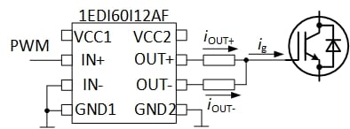
Figure 1: Conventional gate drive using a single IC
Other than more elaborated gate-drive circuits [1], or IPMs [2], the proposed gate-drive system consists of two conventional gate-driver ICs as shown in Figure 1.
Figure 2 shows the proposed gate-drive concept with improved sourcing capability. Two gate drivers of type 1EDI60I12AF are operated in parallel. The input configuration with the terminals IN+ and IN- allows the terminals IN+ to be used for the conventional PWM input signal. The terminal IN- of gate driver IC2 is used to select and deselect the additional output of IC2 by means of an inverted enable-signal /EN. This signal can be simply generated from the application control, or derived from sense signals, which are relevant for switching performance, such as temperature or collector current. Enabling IC2 injects another contribution iOUT+2 to the gate current ig for turn-ON.

Figure 2: Proposed gate drive using two driver ICs for a simple slew-rate control with improved sourcing (top) and sinking (bottom)
Figure 2 depicts that only driver IC1 can be used for turn-OFF. The sinking capability of IC2 cannot be used at the same time, as there could be a condition, where IC1 is sourcing and IC2 is sinking. This would result in excessive power dissipation either in the ICs or in the related gate resistors.
The timing of the gate current ig(t) is shown in Figure 3. The gate current for turn-ON and turn-OFF is provided only by IC1 during low load as shown at the top of Figure 3. The turn-ON performance can be adjusted with respect to the individual application needs or design guidelines, such as the maximum dvCE/dt in drive systems [3]. The change between high-load and low-load operation is done by applying an inverted enable signal to terminal IN- of IC2 according to Figure 2. It activates the sourcing output of IC2 resulting in a faster turn-ON. The value of the additional turn-ON gate resistor at terminal OUT+ of IC2 is selected so that the turn-ON performance of the power transistor again meets the application needs.
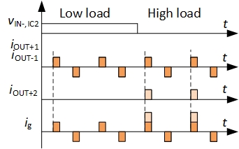
Figure 3: Timing of gate currents for IC1 and IC2 for the proposed gate-drive concept with enforced sourcing
Measurement results’ evaluation
Figure 4 depicts the related results of double-pulse tests for the turn-ON energy Eon and dvCE/dt for various gate resistors and collector currents IC for the gate-drive concept with enforced sourcing. The gate resistors range from 10 Ω up to 47 Ω (solid lines for conventional solution) and the collector currents from 10% up to 100% of the nominal current. The software calculates the 90%/10% value for the dvCE/dt. The tested power transistor is a 40 A / 1200 V IGBT from Infineon (IKW40N120T2).


Figure 4: Effect of the proposed slew-rate control technique on dvCEon/dt (top) and switching energy Eon (bottom) during turn-ON
The voltage slew rate dvCE/dt is continuously increasing over the collector current range. The only exception is the curve representing Rg = 10 Ω at IC = 10 A. Here, a measurement singularity is observed, as the voltage drop over the setup ́s stray inductance triggered the starting condition for the automated dvCE/dt measurement. The same singularity applies to the results of the proposed driver that is depicted by the red dotted line. Two gate drivers with individual gate resistors of Rg1 = 18 Ω and Rg2 = 47 Ω are applied.
The proposed gate-drive technique can use the gate resistor Rg1 in the lower collector current range. It is assumed that the green line representing Rg = 20 Ω in Figure 4 yields similar results as Rg = 18 Ω, and shows rather low dvCE/dt. A changeover to the parallel operation of the two gate-driver ICs with Rg1 = 18 Ω and Rg2 = 47 Ω in parallel may occur in the area of 50% of nominal current (IC = 20 A). The turn-ON energy is shown in the top part of Figure 4. It can be reduced at nominal current (IC = 40 A) from 4.8 mJ down to 3.6 mJ when using the proposed gate drive. This is approximately 25% lower turn-ON energy Eon.
Conclusion
Using two gate drivers per power transistor, combined with a spontaneous selection of the operated gate drivers, is a simple way to enhance the performance of power transistors, since the gate resistors of the two outputs can be dimensioned independently. The use of two gate-drive ICs can be tailored for enforced sourcing capability or enforced sinking capability in a simple way. Furthermore, the use of gate-driver ICs such as Infineon ́s 1EDI60I12AF reduces the design effort compared to discrete solutions with the same functionality. Reductions of the turn-ON energy Eon up to 25% with enforced sourcing can be easily achieved by applying conventional design guidelines. The proposed gate-drive concepts are therefore outperforming conventional approaches.
About the Author
Wolfgang Frank is the principal engineer for product definition and concept of gate driver ICs at Infineon Technologies. Earning his degree in power engineering from Technical University, Munich, he has worked in power engineering for over 20 years.
References
- W. Frank: Real-time adjustable gate current control IC solves dv/dt problems in electric drives, Proc. PCIM 2014
- [Mitsubishi: System Benefits of Using G1 Series Intelligent Power Modules (IPM), Bodo ́s Power Magazine, Edition 3, Germany, 2017
- Gambica Association: Motor Insulation Voltage Stresses Under PWM Inverter Operation, Technical report No.1, third edition, UK, 2006.
This article originally appeared in the Bodo’s Power Systems magazine.