Hello,
I'm going over some projects with friends to study them, as we were told it's a great way to study. Currently, I'm a bit stuck with one of the projects: https://www.pcbway.com/project/shareproject/Desktop_Neon_Effect_LED_Signs_9ae14310.html
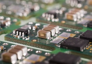
What are some advanced techniques for optimizing power efficiency and reducing EMI/EMC in the circuit design of a neon effect LED sign like the one in the "Desktop Neon Effect LED Signs" project? How can one implement any specific circuit elements or design considerations, such as using a switching power supply or shielding, to address these issues? Also, what measures were taken during the PCB layout to minimize cross-talk and signal interference between the various components and sections of the board?
Thanks in advance!
I'm going over some projects with friends to study them, as we were told it's a great way to study. Currently, I'm a bit stuck with one of the projects: https://www.pcbway.com/project/shareproject/Desktop_Neon_Effect_LED_Signs_9ae14310.html
What are some advanced techniques for optimizing power efficiency and reducing EMI/EMC in the circuit design of a neon effect LED sign like the one in the "Desktop Neon Effect LED Signs" project? How can one implement any specific circuit elements or design considerations, such as using a switching power supply or shielding, to address these issues? Also, what measures were taken during the PCB layout to minimize cross-talk and signal interference between the various components and sections of the board?
Thanks in advance!